SA-1100 Developer’s Manual 10-5
Memory and PCMCIA Control Module
10.1.6 Read-Lock-Write
The read-lock-write sequence is generated by an SWP instruction to a noncacheable/nonbufferable
location. Locked access to memory is ensured through internal arbitration of accesses to the
memory controller.
10.1.7 Aborts and Nonexistent Memory
Reads from reserved address locations (as specified in the memory map) will result in a data abort
exception. Writes to reserved address space will have no effect.
Reads and writes from or to nonexistent memory are not detected in hardware. In case no memory
is selected on a read, the value last driven on the data bus is returned.
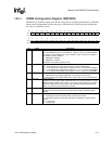
A single access to a disabled DRAM bank (MDCNFG:DEx=0) will cause a CBR refresh cycle to
all banks. Zeros are returned to the register file on reads and writes are dropped. A burst read
access to a disabled DRAM bank will result in a data abort exception.
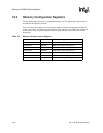
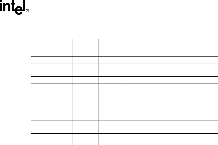
Table 10-1. SA-1100 Transactions
Bus Operation
Burst
Size
Starting
Address
Bits <4:2>
Description
Read single 1 Any Generated by core, DMA, or read buffer request.
Read burst 4 0
4
Generated by read buffer or DMA request.
Read burst 8 0 Generated by cacheline fills or read buffer request.
Write single 1 Any 1..4 bytes are written as specified by the byte mask.
Generated by write buffer or DMA request.
Write burst 2 0, 1, 2
4, 5, 6
All 4 bytes of each word are written. Generated by
write buffer or DMA request.
Write burst 3 0, 1
4, 5
All 4 bytes of each word are written. Generated by
write buffer or DMA request.
Write burst 4 0
4
All 4 bytes of each word are written. Generated by
write buffer or DMA request.
Write burst 8 0 Cacheline copyback. All 32 bytes are written.
Generated by write buffer.


