11-176 SA-1100
Developer’s Manual
Peripheral Control Module
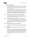
11.12.9.4 Serial Clock Rate (SCR)
The 8-bit serial clock rate (SCR) bit field is used to select the baud or bit rate of the SSP. A total of
256 different bit rates can be selected, ranging from a minimum of 7.2 Kbps to a maximum of
1.8432 Mbps. The serial clock generator uses the 3.6864-MHz clock produced by the on-chip PLL,
divided by a fixed value of 2, and then the programmable SCR value to generate the serial clock
(SCLK). The resultant clock rate is driven out on the SCLK pin and is also used by the SSP’s transmit
logic to drive data out on the TXD4 pin, and latch data on the RXD4 pin. Depending on the frame
format selected, each transmitted bit is either driven on the rising or falling edge of SCLK, and is
sampled on the opposite clock edge. The resultant serial clock rate, given a specific SCR value or
required SCR value given a desired bit rate, can be calculated using the following two respective
equations, where SCR is the decimal equivalent of the binary value programmed within the bit field:
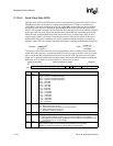
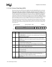
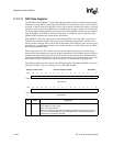
The following table shows the bit locations corresponding to the five different control bit fields
within SSP control register 0. Note that the SSE bit is the only control bit that is reset to a known
state to ensure the SSP is disabled following a reset of the SA-1100. The reset state of all other
control bits is unknown (indicated by question marks) and must be initialized before enabling the
SSP. Reads of bit 6, which is reserved, return zero; writes have no effect.
BitRate
3.6864
6
×10
2x
SCR
1+()
-----------------------------------=
SCR
3.6864
6
×10
2x
BitRate
-------------------------------1–=
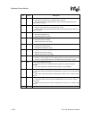
Address: 0h 8007 0060 SSP Control Register 0: SSCR0 Read/Write
Bit1514131211109876543210
SCR SSE
Res. FRF DSS
Reset????????00??????
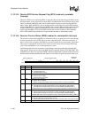
Bit Name Description
3..0 DSS
Data size select.
0000 – Reserved, undefined operation.
0001 – Reserved, undefined operation.
0010 – Reserved, undefined operation.
0011 – 4-bit data.
0100 – 5-bit data.
0101 – 6-bit data.
0110 – 7-bit data.
0111 – 8-bit data.
1000 – 9-bit data.
1001 – 10-bit data.
1010 – 11-bit data.
1011 – 12-bit data.
1100 – 13-bit data.
1101 – 14-bit data.
1110 – 15-bit data.
1111 – 16-bit data.
5..4 FRF
Frame Format.
00 – Motorola SPI frame format.
01 – Texas Instruments
Synchronous serial frame format.
10 – National Microwire frame format.
11 – Reserved, undefined operation.
6—
Reserved.
7SSE
Synchronous serial port enable.
0 – SSP operation disabled, control of pins given to PPC if MCP is also disabled.
1 – SSP operation enabled if MCP disabled or if the PPC SSP pin reassignment bit is set
(reassigns GPIO<13..10> to the SSP).
15..8 SCR
Serial clock rate.
Value (from 0 to 255) used to generate the transmission rate of the SSP.
Bit Rate = 3.6864x10
6
/(2x(SCR+1)), where SCR is a decimal value.


