11-42 SA-1100
Developer’s Manual
Peripheral Control Module
11.7.7 LCD Controller DMA Registers
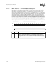
The LCD controller has two fully independent DMA channels used to transfer frame buffer data for
each frame displayed from off-chip memory to the LCD’s palette RAM and the input FIFO. DMA
channel 1 is used for single-panel display mode and the upper screen in dual-panel mode. DMA
channel 2 is used exclusively for the lower screen in dual-panel mode. Both DMA channels contain
a base address pointer and current address pointer register. The LCD’s DMA engine has the highest
priority to gain mastership of the SA-1100’s internal ARM
system bus. The LCD is given highest
priority to prevent other masters from starving the LCD screen (including the CPU).
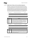
The two DMA channels use a separate set of base address and current address pointers. The user
must initialize the base address pointer registers before enabling the LCD. Once enabled, the base
address is transferred to the current address pointer.
After the LCD is enabled, the input FIFO requests a DMA transfer and the DMA makes a 4-word
burst access from off-chip memory using the address contained within the current address pointer.
The pointer is incremented by 4 (bytes) each time a word is read from memory (bit 2 of the pointer
is incremented). Each of the 4 words from the burst is loaded into the top of the input FIFO. The
LCD then takes one value at a time from the bottom of the FIFO, unpacks it into individual
encoded pixel values, and uses the values to index into the palette. Each time the input FIFO
contains four empty entries, another DMA request is made and another 4-word burst is performed.
To calculate the frame buffer end address, the DMA controller uses the values programmed in the
pixels per line (PPL), lines per panel (LPP), single/dual screen select (SDS), color/monochrome
select (CMS) bit fields, and double pixel data (DPD) bit fields within the control registers as well
as the pixel bit size (PBS) field contained within the first entry of the palette buffer from the
off-chip frame buffer. When the current address pointer reaches the calculated end of buffer
address, the value in the base address pointer is again transferred to the current address pointer.
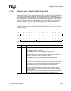
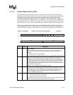
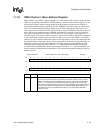
21 HSP Horizontal sync polarity.
0 – L_LCLK pin is active high and inactive low.
1 – L_LCLK pin is active low and inactive high.
Active and passive mode: horizontal sync pulse/line clock active between lines, after
end-of-line wait period.
22 PCP
Pixel clock polarity.
0 – Data is driven on the LCD’s data pins on the rising edge of L_PCLK.
1 – Data is driven on the LCD’s data pins on the falling edge of L_PCLK.
23 OEP
Output enable polarity.
0 – L_BIAS pin is active high and inactive low in active display mode and parallel data
input mode.
1 – L_BIAS pin is active low and inactive high in active display mode and parallel data
input mode.
In active display mode, data is driven out to the LCD’s data pins on programmed pixel
clock edge when ac bias pin is active. Note that OEP is ignored in passive display
mode.
31..24 —
Reserved.
Bit Name Description


