SA-1100 Developer’s Manual 10-1
Memory and PCMCIA Control Module
10
The external memory bus interface for the Intel
®
StrongARM
®
SA-1100 Microprocessor
(SA-1100) supports standard fast-page and EDO asynchronous DRAMs, burst and nonburst
ROMs, Flash EPROMs, SRAM, and PCMCIA expansion devices. It is programmable through the
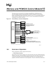
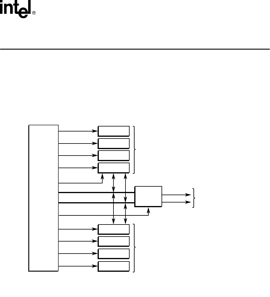
memory interface configuration registers. Figure 10-1 shows a block diagram of the maximum
configuration of the memory controller.
Figure 10-1. General Memory Interface Configuration
10.1 Overview of Operation
The SA-1100 memory interface supports three interfaces:
• DRAM Memory Interface
The dynamic memory interface supports four 32-bit wide banks of fast-page or EDO asynchronous
DRAMs. Each bank is allocated 128 Mbyte of the internal memory map. However, the actual size
of each bank is dependent on the particular DRAM configuration used. If multiple banks are
populated, each must be identical in size and configuration. There are 4 bank selects, nRAS<3:0>,
A6841-01
DRAM Bank 3
DRAM Bank 2
DRAM Bank 1
DRAM Bank 0
RAS3
RAS2
RAS1
DRAM Memory Interface
Up to 4 banks of Standard, EDO,
or Burst EDO DRAM Memory
(32-bits wide)
RAS0
Static Bank 0
Static Bank 1
Static Bank 2
CS0
CS1
CS2
Static Bank 3
CS3
CAS<3:0>
Socket 0
Socket 1
Data Bus
Buffers
and
Transceivers
Address Bus
PCMCIA Control
Intel
®
StrongARM
®*
SA-1100
Memory
Controller
Interface
Static Memory Interface
Up to 4 banks of ROM, Flash, SRAM memory
(16-bit or 32-bit wide)**
** NOTE:
SRAM width is required to be 32 bits.
Static bank 0 must be populated by "bootable" memory
Static RAM support is available in nonRAM systems only.
PCMCIA Interface
Up to 2-socket support.
Requires some
external buffering
* StrongARM is a registered trademark of ARM Limited..


