2-4 SA-1100
Developer’s Manual
Functional Description
2.3 Signal Description
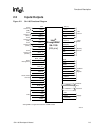
The following table describes the signals.
Key to Signal Types: n – Active low signal
IC – Input, CMOS threshold
ICOCZ – Input, CMOS threshold, output CMOS levels, tristatable
OCZ – Output, CMOS levels, tristatable
Table 2-1. Signal Descriptions (Sheet 1 of 3)
Name Type Description
A<25:0> OCZ Memory address bus. This bus signals the address requested for memory
accesses.
Bits 21..10 carry the 12-bit DRAM address, the static memory devices, and the
expansion bus receive address bits 25..0.
D<31:0> ICOCZ Memory data bus.
nCS<3:0> OCZ Static chip selects. These signals are chip selects to static memory devices such
as ROM and Flash. They are individually programmable in the memory
configuration registers.
nOE OCZ Memory output enable. This signal should be connected to the output enables to
begin driving data onto the data bus.
nWE OCZ DRAM write enable. This signal should be connected to the DRAM write enables
to perform writes. This signal is used in conjunction with CAS<3:0> to perform
byte writes.
nRAS<3:0> OCZ DRAM RAS. These signals should be connected to the DRAM row address strobe
(RAS) pin.
nCAS<3:0> OCZ DRAM CAS. These signals should be connected to the DRAM column address
strobe (CAS) pins.
nPOE OCZ PCMCIA output enable. This PCMCIA signal is an output and is used to perform
reads from memory and attribute space.
nPWE OCZ PCMCIA write enable. This signal is an output and is used to perform writes to
memory and attribute space.
nPIOW OCZ PCMCIA I/O write. This signal is an output and is used to perform write
transactions to the PCMCIA I/O space.
nPIOR OCZ PCMCIA I/O read. This signal is an output and is used to perform read
transactions from the PCMCIA I/O space.
nPCE<2:1> OCZ PCMCIA card enable. These signals are output and are used to select a PCMCIA
card. Bit one enables the high-byte lane and bit zero enables the low-byte lane.
nIOIS16 IC I/O Select 16. This signal is an input and is an acknowledgment from the PCMCIA
card that the current address is a valid 16-bit wide I/O address.
nPWAIT IC PCMCIA wait. This signal is an input and is driven low by the PCMCIA card to
extend the length of the transfers to/from the SA-1100.
PSKTSEL OCZ PCMCIA socket select. This signal is an output and is used by external steering
logic to route control, address, and data signals to one of the PCMCIA sockets.
When PSKTSEL is low, socket zero is selected. When PSKTSEL is high, socket
one is selected. This signal has the same timing as the address lines.
nPREG OCZ PCMCIA register select. This signal is an output and indicates that, on a memory
transaction, the target address is attribute space. This signal has the same timing
as address.
L_DD<7:0> OCZ LCD controller display data.


