


11-160 SA-1100
Developer’s Manual
Peripheral Control Module
11.12.5.2 MCP Data Register 1
When MCP data register 1 (MCDR1) is read, the bottom entry of the telecom receive FIFO is
accessed. As data is removed by the MCP’s receive logic from the incoming data frame, it is placed
into the top entry of the telecom receive FIFO and is transferred down an entry at a time until it
reaches the last empty location within the FIFO. Data is removed by reading MCDR1, which
accesses the bottom entry of the telecom FIFO. After MCDR1 is read, the bottom entry is
invalidated, and all remaining values within the FIFO automatically transfer down one location.
When MCDR1 is written, the topmost entry of the telecom transmit FIFO is accessed. After a
write, data is automatically transferred down to the lowest location within the transmit FIFO,
which does not already contain valid data. Data is removed from the bottom of the FIFO one value
at a time by the transmit logic, is loaded into the correct position within the 64-bit transmit serial
shifter, and then is serially shifted out onto the TXD4 pin during subframe 0.
Telecom data is 14 bits wide and must be left justified by the user before writing it to the transmit
FIFO (MSB of telecom data corresponds to bit 16 of transmit FIFO). The lower two bits of the FIFO
are automatically zero filled by the transmit logic when a 16-bit value is written to MCDR1 for
transmission. The UCB1100 or UCB1200 automatically forces bits 0 and 1 to zero before
transmitting the value to the MCP. The user must right justify received telecom data before using it.
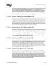
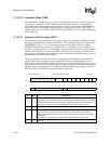
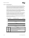
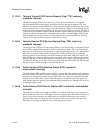
The following table shows MCDR1. Note that the transmit and receive telecom FIFOs are cleared
when the SA-1100 is reset, or by writing a zero to MCE (MCP disabled). Also note that writes to
reserved bits are ignored and reads return zeros.
Address: 0h 8006 000C MCP Data Register 1: MCDR1 Read/Write
Bit 31302928272625242322212019181716
Reserved
Reset0000000000000000
Bit1514131211109876543210
Bottom of Telecom Receive FIFO 0 0
Reset0000000000000000
Read Access
Bit 31302928272625242322212019181716
Reserved
Reset0000000000000000
Bit1514131211109876543210
Top of Telecom Transmit FIFO 0 0
Reset0000000000000000
Write Access
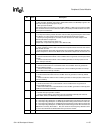
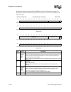
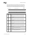
Bit Name Description
1..0 —
Reserved for future enhancements.
Read – Data returned, but UCB1100 or UCB1200 currently zero fills these two bits.
Write – MCP’s transmit logic automatically zero fills these bits.
15..2 Telecom
Data
Transmit/receive telecom FIFO data.
Read – Bottom of telecom receive FIFO data.
Write – Top of telecom transmit FIFO data.
31..16 —
Reserved.