10-24 SA-1100
Developer’s Manual
Memory and PCMCIA Control Module
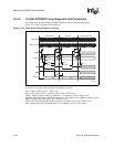
10.4.6 FLASH EPROM Timing Diagrams and Parameters
Flash reads have the same timing as nonburst ROMs as shown in the preceding figures.
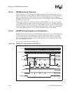
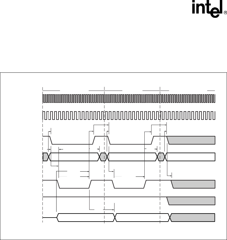
Figure 10-10 shows the timing for Flash writes.
In Figure 10-10, some of the parameters are defined as follows:
tAS = Address setup to nCS = 1 CPU cycle
tCES = nCS setup to nWE = 2 memory clock cycles (4 CPU cycles)
tASW = Address setup to nWE low (asserted) = 2-1/2 memory cycles (5 CPU cycles)
tDSWH = Write data setup to nWE high (deasserted) = 1/2 memory cycle + (RDN+1) memory cycles
tDH = Data hold after nWE high = 1+1/2 memory cycle
tCEH = nCS held asserted after nWE deasserted = 1 memory clock cycle (2 CPU cycles)
tAH = Address hold after nWE deasserted = 1+1/2 memory cycle (3 CPU cycles)
Figure 10-10. Flash Write Timing Diagram (2 Writes)
A4787-01
CPU Clock
Memory Clock
A[25:0]
D[31:0]
nWE
nOE
nCS0
RDN+1
(2*RRR)+1 (2*RRR)+1
tAS
tAS
tASW
tCES
tDH
tCES
tCEH tCEH
tAHtAH
Write Command Write Data Possible Read or Write
tCES
tAS
RDN+1
tDSWH
A0
CMD DATA


