SA-1100 Developer’s Manual 5-3
Coprocessors
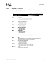
5.2.2 Register 1 – Control
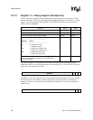
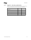
Register 1 is a read/write register containing control bits. All writable bits in this register are forced
low by reset. The shaded bits (also labeled r) are reserved and are not readable or writable.
M bit 0 Enable/disable
0 – On-chip memory-management unit disabled
1 – On-chip memory-management unit enabled
A bit 1 Address fault enable/disable
0 – Alignment fault disabled
1 – Alignment fault enabled
C bit 2 Data cache enable/disable
0 – Data cache disabled
1 – Data cache enabled
W bit 3 Write buffer enable/disable
0 – Write buffer disabled
1 – Write buffer enabled
B bit 7 Big/little endian
0 – Little endian operation
1 – Big endian operation
S bit 8 System
This bit selects the access checks performed by the memory-management unit.
See the
ARM Architecture Reference
for more information.
R bit 9 ROM
This bit selects the access checks performed by the memory-management unit.
See the
ARM Architecture Reference
for more information.
I bit 12 Instruction cache enable/disable
0 – Instruction cache disabled
1 – Instruction cache enabled
X bit 13 Virtual interrupt vector adjust
0 – Base address of interrupt vectors is 0h0000 0000
1 – Base address of interrupt vectors is 0hFFFF 0000
Bits 14..31 Unused.
Undefined on Read. Writes ignored.
rrrrrrrrrrrrrrrrrrXIrrRSB111W ACM
012345678931
12
13


