11-104 SA-1100
Developer’s Manual
Peripheral Control Module
11.10.1 Low-Speed ICP Operation
Following reset, both the UART and HSSP are disabled, which causes the peripheral pin controller
(PPC) to assume control of the port’s pins. Reset causes the PPC to configure all of the peripheral
pins as inputs, including serial port 2’s transmit (TXD2) and receive (RXD2) pins. Reset also
causes the UART’s transmit and receive FIFOs to be flushed (all entries invalidated). Before
enabling the ICP for low-speed operation, the user must first clear any writable or “sticky” status
bits, which are set by writing a one to each bit. Next, the desired mode of operation is programmed
in the control registers. At this point the user may “prime” the UART’s transmit FIFO by writing up
to eight values, or the FIFO can remain empty and either programmed I/O or the DMA can be used
to service it after the ICP is enabled. Once the ICP is enabled, transmission/reception of data can
begin on the transmit (TXD2) and receive (RXD2) pins.
For low-speed operation, all serial data that is transferred between the TXD2/RXD2 pins and the
ICP’s UART is modulated/demodulated according to the HP-SIR IrDA standard. The IrDA
standard also specifies the frame format that must be used by the UART.
11.10.1.1 HP-SIR
*
Modulation
Hewlett-Packard Serial Infrared
*
(SIR) modulation is used for low-speed transmission up to
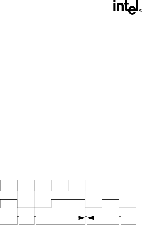
115.2 Kbps. Logic zero is represented by a pulse of light that is either 3/16 of the bit time wide, or
1.6 µs wide (1.6 µs is 3/16 of the bit time for the highest bit rate of 115.2 Kbps). The rising edge of
the pulse corresponds to the start of the zero bit time. Logic one is represented by the absence of
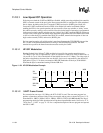
light pulses. Figure 11-24 shows an example of HP-SIR modulation of the byte, 8’b01011001.
Note that the byte is transmitted starting with the LSB first.
11.10.1.2 UART Frame Format
For transmission rates up to 115.2 Kbps, the ICP’s UART is used. The user must program it to
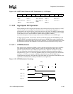
produce a frame that produces 8 bits of data, one stop bit, and no parity, as shown in Figure 11-25.
Note that PE=1, SBS=1, DSS=0, SCE=1, BRK=1, RXE=0, TXE=0, and BRD=0x000 are illegal
programming modes for IrDA operation and will produce unpredictable results. See Section 11.11,
“Serial Port 3 - UART” on page 11-128 for a complete description of how to program and operate
the ICP’s UART.
Figure 11-24. HP-SIR Modulation Example
Digital
Data
HP-SIR
*
Data
Bit
Value
10011010
3/16 of the Bit Time
LSB
MSB


