10-18 SA-1100
Developer’s Manual
Memory and PCMCIA Control Module
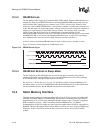
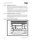
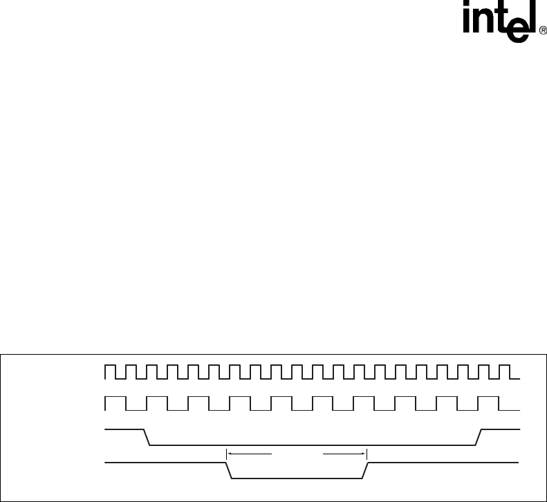
10.3.3 DRAM Refresh
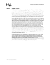
The SA-1100 provides support for CAS before RAS (CBR) refresh. When the DRAM interface is
enabled [by setting any of MDCNFG:DE(3-0) and setting MDCNFG:DRI greater than zero], the
refresh counter starts counting up every memory cycle (2 CPU cycles) from 0. When its value
reaches the value in MDCNFG:DRI times 4, the memory controller is notified that a refresh cycle
is due, then the counter is cleared and resumes counting. After the current transaction completes, a
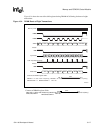
refresh cycle is performed. All four nCAS lines are asserted. Two memory clock cycles later
(4 CPU cycles), the nRAS signals for all enabled banks are asserted and held low for
MDCNFG:TRASR+1 memory clock cycles. After that, all nRAS and nCAS signals are deasserted
and MDCNFG:TRP is used to hold off subsequent DRAM accesses to allow for row precharge
time. Hardware reset clears the refresh counter. Software reset does not affect it.
A read or write to any disabled DRAM bank will cause a refresh cycle to all banks to occur.
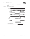
Figure 10-5 shows a timing diagram of a CBR refresh cycle.
10.3.4 DRAM Self-Refresh in Sleep Mode
The SA-1100 will put the DRAM into the self-refresh state prior to entering sleep mode by
asserting nCAS, then asserting nRAS (just as for a normal CBR refresh cycle), and maintaining
nCAS and nRAS low while power and clocks are turned off.
See Section 9.5, “Power Manager” on page 9-26 for details on how to bring the DRAMs out of
self-refresh mode. An access to a DRAM bank while the DRAM interface is in self-refresh mode
will have undefined results, but the DRAMs will remain in self-refresh mode.
10.4 Static Memory Interface
The static memory interface is comprised of four chip selects, nCS<3:0>, and are each configurable
for ROM, burst ROM, SRAM, or Flash EPROM. The data bus for each chip select region may be
programmed to be 16 or 32 bits wide, although if SRAM is selected, only a 32-bit bus is supported.
nOE is asserted for all reads. nWE is asserted for Flash and SRAM writes. For SRAM
implementations, nCAS<3:0> signals are used for the byte enables where nCAS<3> corresponds to
the MSB. The SA-1100 supplies 26 bits of byte address (A<25:0>) for access of up to 128 Mbyte per
chip select. A<0> is not used in 16-bitwide bus systems and <1:0> are not used in 32-bitwide
systems.
Figure 10-5. DRAM Refresh Cycle
A4779-01
CPU Clock
Memory Clock
TRASR+1
nCAS[3:0]
nRAS[3:0]


