11-110 SA-1100
Developer’s Manual
Peripheral Control Module
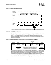
At the end of each frame transmitted, the HSSP outputs a pulse called the serial infrared interaction
pulse (SIP). A SIP is required at least every 500 ms to keep slower speed devices (115.2 Kbps and
slower) from colliding with the higher speed transmission. The SIP simulates a start bit that causes
all low-speed devices to stay off the bus for at least another 500 ms. Transmission of the SIP pulse
causes the TXD2 pin to be forced high for a duration of 1.625 µs and low for 7.375 µs (total SIP
period = 9.0 µs). After the 9.0 µs elapses, the preamble is then transmitted continuously to indicate
to the off-chip receiver that the HSSP’s transmitter is in the idle state. The preamble continues to be
transmitted until new data is available within the transmit FIFO, or the HSSP’s transmitter is
disabled. Note that it is the responsibility of the user to ensure that a frame completes once every
500 ms such that a SIP pulse is produced, keeping all low-speed devices from interrupting
transmission. Because most IrDA compatible devices produce a SIP after each frame transmitted,
the user only needs to ensure that a frame is either transmitted or received by the ICP every 500 ms.
Note that frame length does not represent a significant portion of the 500 ms timeframe in which a
SIP must be produced. At 4.0 Mbps, the longest frame allowed is 16,568 bits, which takes just over
4 ms to transmit. Also note that the HSSP issues a SIP when the transmitter is first enabled to
ensure all low-speed devices are silenced before transmitting its first frame.
If the user disables the HSSP’s transmitter during operation, transmission of the current data byte is
stopped immediately, the serial shifter and transmit FIFO are cleared, control of the TXD2 pin is
given to the peripheral pin control (PPC) unit, and all clocks used by the transmit logic are
automatically shut off to conserve power. The user should ensure that the polarity of the TXD2
output is reprogrammed properly if this pin is to be used as a GPIO output.
11.10.2.10 Transmit and Receive FIFOs
To reduce chip size and power consumption, the HSSP’s FIFOs use self-timed logic (they are not
clocked). Because of process and environmental variations, the depth at which a service request is
triggered to empty the receive FIFO is variable. This variation spans a maximum of four FIFO
entries; the receive FIFO service request can be made at four different FIFO depths.To compensate
for this variability and guarantee that at least eight valid entries of data exist within the FIFO before
generating a service request, an extra four entries have been added to the receive FIFO ( four
entries more than the transmit FIFO). The transmit FIFO is 16 entries deep and the receive FIFO is
20 entries deep. The point at which the receive FIFO service request is triggered spans one fifth
(four entries) of the 20-entry FIFO. The service request is signalled at a depth from two-fifths full
to three-fifths full (when the FIFO contains nine, ten, eleven, or twelve entries of data).
This service request variation applies only to an empty FIFO that is filled (receive FIFO). It does
not apply to a full FIFO that is emptied (transmit FIFO). The transmit FIFO is guaranteed to signal
a service request when it has eight or more empty entries and negate the request when the FIFO
contains nine or more entries that are filled.
If the DMA is used to service either one or both of the HSSP’s FIFOs, the burst size must be set to
eight words, even though more than eight entries of data may exist within the receive FIFO. If
programmed I/O is used to service the FIFOs, a maximum of 8 words may be added to the transmit
FIFO without checking if more space is available. Likewise, a maximum of 8 words may be
removed from the receive FIFO without checking if more data is available. After this point, the
user must poll a set of status bits that indicate if any data remains in the receive FIFO or if space is
available in the transmit FIFO before emptying or filling the FIFOs any further.
11.10.2.11 CPU and DMA Register Access Sizes
Bit positioning, byte ordering, and addressing of the SDLC is described in terms of little endian
ordering. All ICP (HSSP and UART) registers are 8 bits wide and are located in the least
significant byte of individual words. The ARM
peripheral bus does not support byte or half-word


