


SA-1100 Developer’s Manual 11-161
Peripheral Control Module
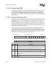
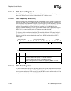
11.12.5.3 MCP Data Register 2
MCDR2 contains 21 bits and is used to perform reads and writes to any of the UCB1100’s or
UCB1200’s registers. MCDR2 contains three separate fields: MCDR2<15:0> is the 16-bit register
data field, MCDR2<16> is a 1-bit read/write control bit, and MCDR2<20:17> is the 4-bit register
address field. A value written to MCDR2 is placed in the correct position within the 64-bit
subframe 0, is transmitted to the off-chip codec, and is used to perform a read or write operation to
the addressed codec register. Note that the contents of the addressed register are always returned in
the receive data frame and placed in the MCDR2 regardless of the state of the read/write bit. Thus
for write cycles, both a write and a read occurs, and for read cycles, only a read occurs. When
MCDR2 is read, the value returned from the last read or write operation, which was completed to
the codec, is returned.
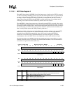
A register write is performed by writing the correct value to each of the three fields within MCDR2
using one 16- or 32-bit write, ensuring that the read/write bit is set. Its contents are then transferred
to the correct fields within the serial shifter on the next rising edge of the SFRM signal, and then to
the codec via the TXD4 pin during subframe 0. The value within MCDR2<15:0> is written to the
selected codec register at the end of subframe 0 (during the 65th bit of the frame). The data written
to the control register and its address is returned to the MCP during the next data frame, and is
placed back within MCDR2 with the read/write bit reset to zero. For a write operation, since the
addressed register is written at the end of subframe 0, the data returned during the frame in which
the write occurred represents the previous contents of the register. The updated value is returned
during the next data frame.
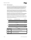
A register read is performed by writing the address of the register to read while clearing the
read/write bit to zero within MCDR2. Again, the data is transferred to the serial shifter on the next
rising edge of the SFRM signal and is transmitted to the UCB1100 or UCB1200 during subframe 0.
Because the address and read/write control bit fields are placed near the beginning of the serial
stream output, the codec performs the read immediately after the read/write bit is received (during
the 41st bit of the frame), and the value contained within the addressed register is sent back to the
MCP in the same data frame, and is placed within MCDR2.
Once MCDR2 is written with a value to execute a read or write, the operation is performed every
MCP data frame until a new value is written to the register. Thus continual reads or writes are made
to the addressed codec register until a new read or write operation is configured.