11-46 SA-1100
Developer’s Manual
Peripheral Control Module
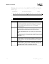
11.7.11 LCD Controller Status Register
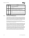
The LCD controller status register (LCSR) contains bits that signal overrun and underrun errors for
both the input and output FIFOs, ac bias pin transition count, LCD disabled, DMA base update
ready, and DMA transfer bus error conditions. Each of these hardware-detected events signal an
interrupt request to the interrupt controller.
Each of the LCD’s status bits signal an interrupt request as long as the bit is set. Once the bit is
cleared, the interrupt is cleared. Read/write bits are called status bits (read-only bits are called
flags). Status bits are referred to as “sticky” (once set by hardware, they must be cleared by
software). Writing a one to a sticky status bit clears it; writing a zero has no effect. Read-only flags
are set and cleared by hardware; writes have no effect. The user has the ability to mask all LCD
interrupts by clearing bit 12 within the interrupt controller mask register (ICMR). See the
Section 9.2, “Interrupt Controller” on page 9-11.
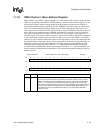
11.7.11.1 LCD Disable Done Flag (LDD) (read/write, maskable interrupt)
The LCD disable done flag (LDD) is set after the LCD has been disabled and the frame that is
active finishes being output to the LCD’s data pins. When the LCD is disabled by clearing the LCD
enable bit
(LEN= 0 → 1) in LCCR0, the LCD allows the current frame to complete before it is
disabled. After the last set of pixels is clocked out onto the LCD’s data pins by the pixel clock, the
LCD is disabled, LDD is set, and an interrupt request is made to the interrupt controller if it is
unmasked (LDM=0). This interrupt is useful to allow an orderly shutdown of the LCD controller
before the user places the SA-1100 into sleep mode.
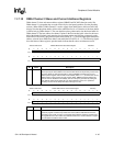
11.7.11.2 Base Address Update Flag (BAU) (read-only, maskable interrupt)
The base address update flag (BAU) is a read-only bit that is set after the contents of the DMA base
address register 1 are transferred to the DMA current address register 1 and is cleared when DMA
base address register 1 is written. The value in the base address register is transferred to the current
address register when the LCD is first enabled by writing a one to LEN
(LEN= 0 → 1) and when the
current address pointer equals the end address value calculated by the LCD controller. When BAU
is set, an interrupt request is made to the interrupt controller if it is unmasked (BAM = 0). This
interrupt allows the user to program the DMA with a new base address value to alternate between
two or more frame buffer locations. When dual-panel mode is enabled (SDS=1), both DMA
channels are enabled, and BAU is set only after both channels’ base address registers are
transferred to their corresponding current address registers (1 and 2) and is cleared when DMA
base address register 2 (lower panel) is written. Therefore, the user must always update the DMA
base address register 1 (upper panel) first in dual-panel mode.
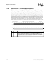
11.7.11.3 Bus Error Status (BER) (read/write, maskable interrupt)
The bus error status (BER) bit is set when a DMA transfer causes a bus error to occur on the ARM
system bus. A bus error is signalled when the DMA controller attempts to access a reserved or
nonexistent memory space. When this occurs, the SA-1100’s memory controller returns zeros for
the read. It asserts the bus error signal to the LCD’s DMA, which in turn, causes the BER bit to be
set and an interrupt request is made to the interrupt controller if it is unmasked (ERM = 0). The
DMA is not disabled as a result of the bus error and operation continues as normal. If a DMA
access causes a bus error, zeros are returned by the memory controller, which causes a palette entry
to be filled with zeros (highest intensity color or black), or if pixel data is being DMAed, the LCD
accesses the first location of the palette RAM one or more times.


