SA-1100 Developer’s Manual 11-169
Peripheral Control Module
11.12.7 SSP Operation
Following reset, both the MCP and SSP logic within serial port 4 is disabled and control of its pins is
given to the PPC that configures all four pins as inputs. To enable SSP operation, the programmer
should first clear any interruptible status bits, which are set following the reset by writing a one to
them. Next, the user should program the SSP’s control registers with the desired mode of operation,
ensuring that the register containing the SSP enable bit is programmed last. Note that the MCP has
precedence over the SSP and must be disabled first before enabling the SSP. The user can choose to
either “prime” the transmit FIFO by writing up to eight 16-bit values, or allow the transmit FIFO
service request to interrupt the CPU or trigger a DMA transfer to fill the FIFO. Once enabled,
transmission/reception of data begins on the transmit (TXD4) and receive (RXD4) pins, and is
synchronously controlled by the serial clock (SCLK) and serial frame (SFRM) pins.
11.12.7.1 Frame Format
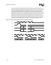
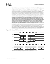
Each data frame is between 4 and 16 bits long depending on the size of data programmed, and is
transmitted starting with the MSB. There are three basic frame types that can be selected: Motorola*
SPI, Texas Instruments* synchronous serial, and National Microwire*. For all three formats, the
serial clock (SCLK) is held low or inactive, while the SSP is idle and transitions at the programmed
frequency only during active transmission of data. For Motorola* SPI and National Microwire*
frame formats, the serial frame (SFRM) pin is active low, and is asserted (pulled down) during the
entire frame’s transmission. In these modes, the SFRM pin is used to select the off-chip slave serial
device, enabling it for transmission. For Texas Instruments* format, the SFRM pin is pulsed for one
serial clock period starting at its rising edge, prior to each frame’s transmission. The type of serial
clock edges used to drive and sample data are different for all three modes. For National Microwire*
format, both the SSP and the off-chip slave device drive their output data on the falling edge of
SCLK, and latch data from the other device on the rising edge. For Texas Instruments* format, both
the SSP and the off-chip slave device drive their output data on the rising edge of SCLK, and latch
data from the other device on the falling edge. For Motorola* SPI format, the user has the option of
which edge of SCLK to drive and sample data, as well as the phase of the SCLK signal (whether it is
shifted one-half period to the left or right during the frame transmission).
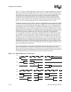
Unlike the full-duplex transmission of the other two frame formats, the National Microwire
*
format uses a special master-slave messaging technique that operates at half-duplex. In this mode,
when a frame begins, an 8-bit control message is transmitted to the off-chip slave. During this
transmit, no incoming data is received by the SSP. After the message has been sent, the off-chip
slave decodes it and responds with the requested data after waiting one serial clock after the last bit
of the 8-bit control message has been sent. The returned data can be 4 to 16 bits in length, making
the total frame length anywhere from 13 to 25 bits.


