11-158 SA-1100
Developer’s Manual
Peripheral Control Module
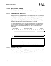
11.12.4 MCP Control Register 1
The MCP control register 1 (MCCR1) contains one bit that selects one of two fixed frequencies to
drive the MCP. Note that this register resides within the PPC’s address space.
11.12.4.1 Clock Frequency Select (CFS)
When the on-chip clock is enabled (ECS=0), the clock frequency select (CFS) bit is used to select
either a 9.585-MHz or an 11.981-MHz clock to drive the MCP’s serial clock rate. When ECS=0
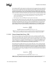
and CFS=0, the on-chip 3.6864-MHz oscillator is first multiplied by 13 then divided by 4, resulting
in an 11.9808-MHz bit clock frequency. When ECS=0 and CFS=1, the on-chip 3.6864 MHz
oscillator is first multiplied by 13 then divided by 5, resulting in a 9.58464-MHz bit clock
frequency. Note that when ECS=1, CFS is ignored and an external clock is input to the MCP via
GPIO pin 21. Also note that CFS is cleared following a reset of the SA-1100 so that the MCP
defaults to 11.981-MHz operation, which is standard for the UCB1100/1200.
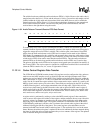
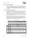
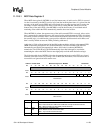
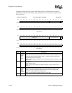
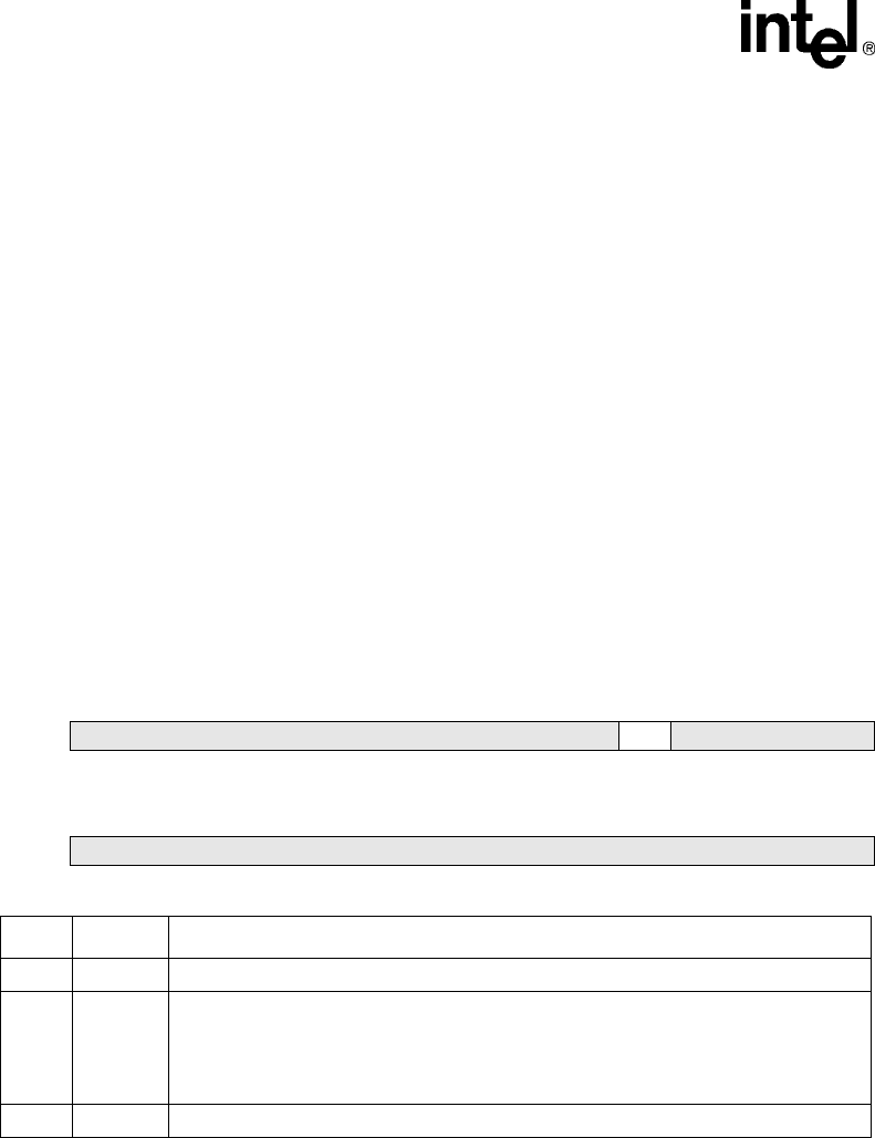
The following table shows the location of the CFS control bit within the MCP control register 1.
The CFS is cleared to zero selecting 11.981-MHz operation following a reset of the SA-1100.
Writes to reserved bits are ignored and reads return zeros. MCCR1 resides within the PPC’s
address space.
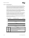
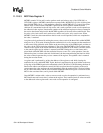
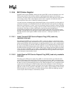
11.12.5 MCP Data Registers
The MCP contains three data registers. MCDR0 addresses the top entry of the audio transmit FIFO
and bottom entry of the audio receive FIFO, MCDR1 addresses the top and bottom entries of the
telecom transmit and receive FIFOs respectively, and MCDR2 is used to perform reads and writes
to any of the codec’s 16 registers via the MCP’s serial interface.
Address: 0h 9006 0030 MCP Control Register 1: MCCR1 Read/Write
Bit 31302928272625242322 212019181716
Reserved CFS Reserved
Reset0000000000 000000
Bit 151413121110 9 8 7 6 5 4 3 2 1 0
Reserved
Reset0000000000 000000
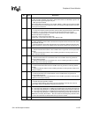
Bit Name Description
19..0 —
Reserved.
20 CFS
Clock frequency select.
0 – If ECS=0, bit rate clock frequency of 11.981 MHz is selected.
1 – If ECS=0, bit rate clock frequency of 9.585 MHz is selected.
If ECS=1, CFS is ignored and an external clock supplied by GPIO pin 21 is used.
31..21 —
Reserved.


