SA-1100 Developer’s Manual 10-33
Memory and PCMCIA Control Module
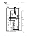
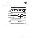
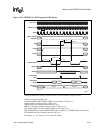
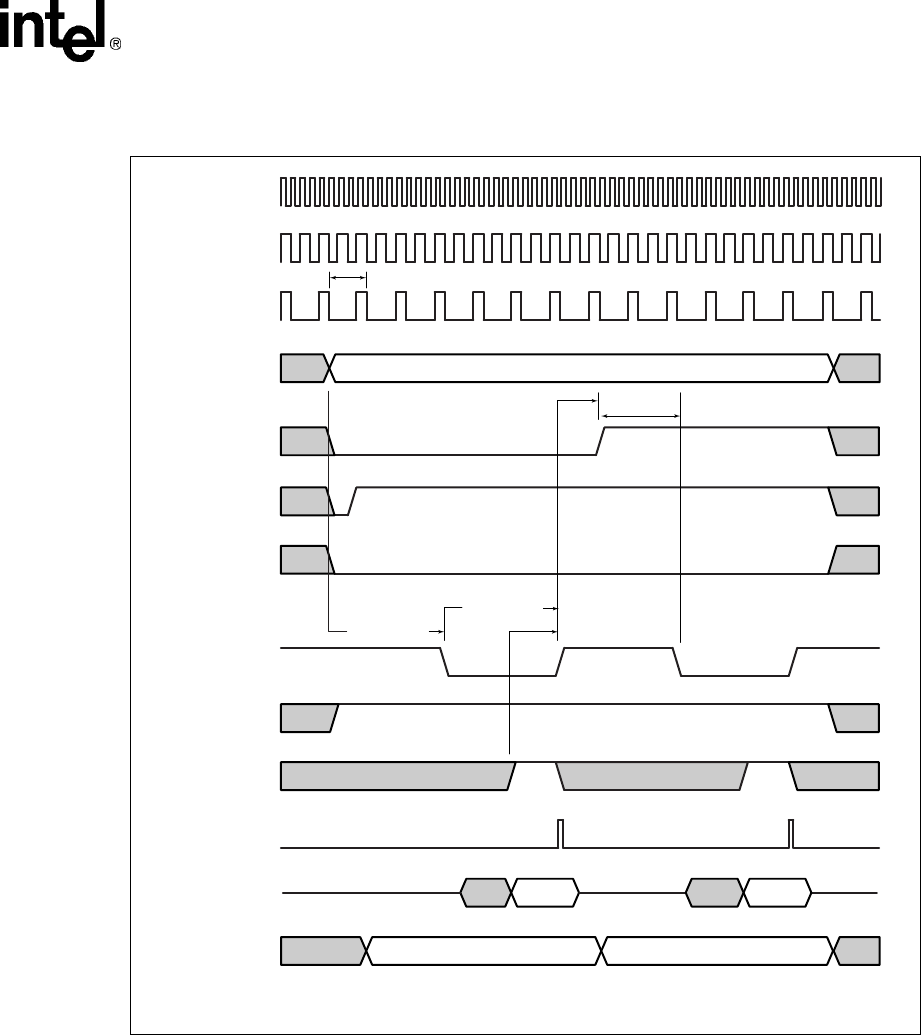
Timing parameters are in CPU clock cycle units. All are minimums except as noted:
Address access time: 6*(BS_xx+1)
Command (nPOE, nPWE, nPIOR, nPIOW) assertion time: 3*(BS_xx+1)
Address setup to command assert: 3*(BS_xx+1)
Address hold after command deassertion: BS_xx+1
nPWAIT valid after command assertion (max): 2*(BS_xx+1) -1
Chip enable (nPCE1,2) setup to nPOE, nPWE assert: 3*(BS_xx+1)
Chip enable (nPCE1,2) setup to nPIOR, nPIOW assert: 3*(BS_xx+1) - (nIOIS 16 delay from address)
Chip enabled hold from command deassert: BS_xx+1
See Chapter 13, “AC Parameters” for actual AC timing.
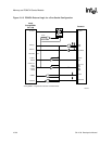
Figure 10-16. PCMCIA I/O 16-Bit Access to 8-Bit Device
A4788-01
CPU Clock
Memory Clock
BS_xx+1
BS_xx+1
BS_xx+2
2*(BS_xx+1)
3*(BS_xx+1)
3*(BS_xx+1)
BCLK
A[0]
A[25:1], nPREG,
PSKTSEL
nPCE2
nPIOR, nPIOW
nIOIS16
nPWAIT
Read Data
D[7:0]
Write Data
D[7:0]
BS_xx = 1
Latch Read
Data
nPCE1
Low Byte High Byte
High ByteLow Byte


