


SA-1100 Developer’s Manual 11-111
Peripheral Control Module
operations. All reads and writes of the ICP by the CPU should be wordwide. Two separate,
dedicated DMA requests exist for both the transmit and the receive FIFOs. If the DMA controller is
used to service the transmit and/or receive FIFOs, the user must ensure the DMA is properly
configured to perform bytewide accesses, using 8 bytes per burst for the HSSP and 4 bytes per
burst for the UART. See later sections in this chapter for summaries of the ICP’s UART registers
and HSSP registers.
11.10.3 UART Register Definition
The ICP’s UART is the same as serial port 3’s UART except that one additional register exists to
control HP-SIR modulation for low-speed operation. See Section 11.11, “Serial Port 3 - UART” on
page 11-128 for a description of the programming and operation of all other features of the ICP’s
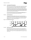
UART. Note that the user must ensure that the UART is programmed to yield the frame format
shown in Figure 11-25.
11.10.4 UART Control Register 4
UART control register 4 (UTCR4) contains two different bit fields that control various functions
for 115.2-Kbps (low-speed) IrDA transmission.
11.10.4.1 HP-SIR Enable (HSE)
The HP-SIR enable (HSE) bit controls whether the HP-SIR bit modulation logic is enabled or
disabled. When HSE=0, HP-SIR modulation is disabled, and if UART operation is enabled
(ITR=0), it is used for normal serial transmission (NRZ encoding only) rather than IrDA
communication. When HSE=1, HP-SIR modulation is enabled for low-speed IrDA
communication; zeros are represented by pulses that are 3/16 of the programmed bit width, while
ones are represented by no pulses.
11.10.4.2 Low-Power Mode (LPM)
The low-power mode (LPM) bit controls whether the HP-SIR bit modulation logic represents zeros
using a pulse that is 3/16 of the chosen bit width or a fixed 1.6 µs pulse width. When LPM=0, zeros
are encoded as a pulse, which is 3/16 of the bit width programmed within the UART’s baud rate
divisor (BRD) bit field. When LPM=1, the UART’s programmed bit length is ignored and zeros are
represented by pulses that are 1.6 µs in duration. Programming LPM=1 minimizes the time that the
off-chip LED transceiver is turned on to the minimum pulse width specified by the IrDA low-speed
standard, which in turn, minimizes power consumption.
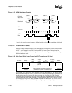
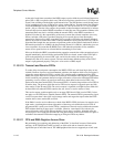
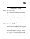
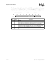
The following table shows the location of the bits within UART control register 4; question marks
indicate that the values are unknown at reset. Both bits are reset to zero. Note that the UART must
be disabled (RXE=TXE=0) when changing the state of either of these two bits. Also note that
writes to reserved bits are ignored and reads return zeros.
Address: 0h 8003 0010 UTCR4 Read/Write
Bit 7 6 5 4 3 2 1 0
Reserved LPM HSE
Reset 0 0 0 0 0 0 ? ?