


9-36 SA-1100
Developer’s Manual
System Control Module
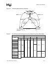
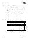
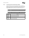
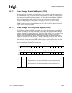
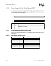
9.5.7.4 Power Manager Wake-Up Enable Register (PWER)
The following table shows the location of all wake-up interrupt enable bits in the PWER. For a
GPIO to serve as a wake-up source, it must be programmed as an input in the GPDR. When a fault
condition is detected in the VDD_FAULT or BATT_FAULT pins, this register is set to hexadecimal
0000 0003, enabling only GP<1,0> as wake-up sources. This register is also set to this value on
hard reset (nRESET asserted). For reserved bits, writes are ignored and reads return zero.
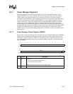
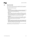
Bit31302928272625242322212019181716
R/W
WE31 Reserved WE27 WE26 WE25 WE24 WE23 WE22 WE21 WE20 WE19 WE18 WE17 WE16
Reset0000000000000000
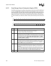
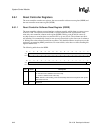
Bit1514131211109876543210
R/W
WE15 WE14 WE13 WE12 WE11 WE10 WE9 WE8 WE7 WE6 WE5 WE4 WE3 WE2 WE1 WE0
Reset0000000000000011
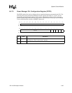
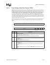
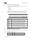
Bit Name Description
{n} WE{n}
Sleep wake-up enable n (where n = 0 through 27).
0 – Wake-up due to GPIO<n> edge detect disabled.
1 – Wake-up due to GPIO<n> edge detect enabled.
30..28 —
Reserved.
31 WE31
Sleep wake-up enable 31.
0 – Wake-up due to RTC alarm disabled.
1 – Wake-up due to RTC alarm enabled.