11-88 SA-1100
Developer’s Manual
Peripheral Control Module
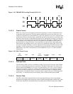
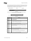
11.9.4 SDLC Control Register 1
SDLC control register 1 (SDCR1) contains eight bit fields that control various functions within the
SDLC.
11.9.4.1 Abort After Frame (AAF)
The abort after frame (AAF) bit controls whether or not the SDLC transmits an abort at the end of
each frame transmitted, and also controls the state of GPIO pin 17. When the AAF bit is set, each
time the SDLC completes transmission of the flag at the end of a frame, the transmit logic signals
an abort by transmitting 12 sequential ones on the transmit pin (TXD1). Additionally, any time the
transmitter is idle (not sending a frame or the abort at the end of the frame), the SDLC forces GPIO
pin 17 high. Likewise, when the SDLC is actively transmitting a frame (including the start and stop
flags, and the abort at the end of the frame), it forces GPIO pin 17 low. If the transmit FIFO is
emptied at the end of a frame, the abort is signalled followed by the continuous transmission of
flags. If there is data present within the FIFO (indicating a new frame is available), the abort is
followed by the programmed number of start flags, then data transmission begins again. For this
case, GPIO<17> is not asserted because the two frames occur back-to-back (no idle time between
the two frames). Note that the user must configure GPIO<17> as an output by setting the pin
direction bit for pin 17 within GPDR. When AAF=1, the state of GPIO<17> is controlled solely by
serial port 1. Writing to the pin set (GPSR) or pin clear (GPCR) registers for pin 17 has no effect.
See Chapter 9, “System Control Module” for a description of GPIO programming.
4SCESample clock enable.
0 – On-chip baud rate generator and digital PLL used to transmit and receive SDLC data.
1 – A clock is input or output via GPIO pin 16 and is used to synchronously sample
receive data and drive transmit data.
Note: BMS must be programmed to select NRZ encoding when sample clock operation is
enabled (BMS=1).
5SCD
Sample clock direction.
0 – If sample clock enabled, it is input using GPIO pin 16.
1 – If sample clock enabled, the sample clock generated by the programmable baud rate
generator but before the fixed divide by 16 is output using GPIO pin 16.
Note: For both directions, the sample clock is used to synchronously sample receive data
and drive transmit data on the edges selected using RCE and TCE. A maximum of
3.6864-MHz clock allowed.
6 RCE
Receive clock edge select.
0 – Rising edge of clock input/output on GPIO pin 16 used to latch data from the receive pin.
1 – Falling edge of clock input/output on GPIO pin 16 used to latch data from the receive pin.
7TCE
Transmit clock edge select.
0 – Rising edge of clock input/output on GPIO pin 16 used to drive data onto the transmit pin.
1 – Falling edge of clock input/output on GPIO pin 16 used to drive data onto the transmit pin.


