


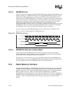
10-26 SA-1100
Developer’s Manual
Memory and PCMCIA Control Module
10.6 PCMCIA Overview
The SA-1100 PCMCIA interface provides controls for one PCMCIA card slot with a PSKTSEL
pin for support of a second slot. This 16-bit host interface supports 8- and 16-bit peripherals and
handles common memory, I/O, and attribute memory accesses. The interface does not support the
PCMCIA DMA protocol. The duration of each access is based on an internally generated clock that
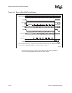
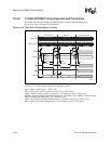
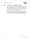
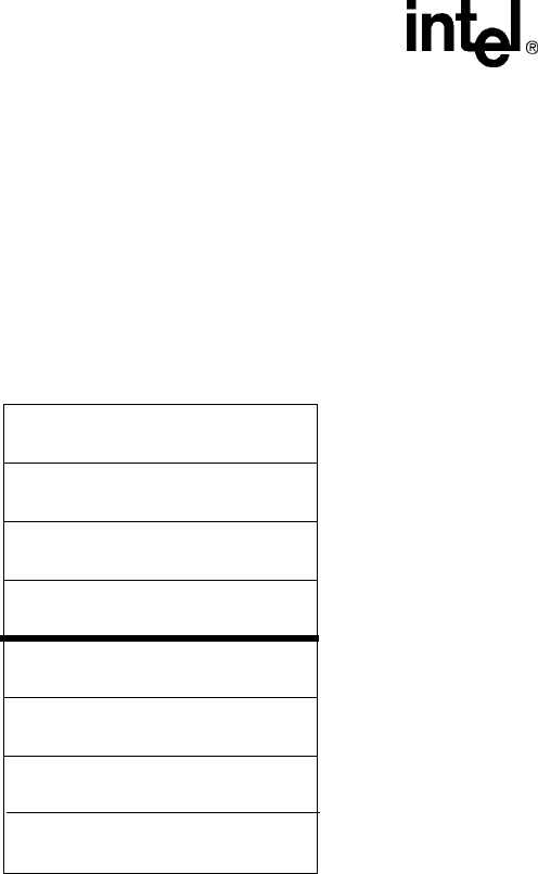
is programmed per address space in the MECR register. Figure 10-11 shows the memory map for
the PCMCIA space.
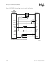
The PCMCIA memory space is divided into eight partitions, four for each card slot. The four
partitions for each card slot are common memory, I/O, attribute memory, and a reserved space.
Each partition starts on a 64 Mbyte boundary. Pins A<25:0>, nPREG, and PSKTSEL are driven at
the same time. nPCE1 and nPCE2 are driven at address time for memory and attribute accesses.
For I/O accesses, their value depends on the value of nIOIS16 and thus will be valid a finite time
after nIOIS16 is valid.
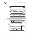
Common memory accesses assert the nPOE or nPWE control signals and are always 16-bit
accesses with nPCE1 asserted for low byte access and nPCE2 asserted for high byte access. I/O
accesses assert the nIOR or nIOW control signals and use the nIOIS16 input signal to determine
the bus width of the transfer (8 or 16 bit). The SA-1100 uses nPCE2 to indicate to the expansion
device that the upper half of the data bus, D<15:8>, will be used for the transfer and nPCE1 to
indicate that the lower half of the data bus, D<7:0>, will be used. When nPCE2 is low, A<0> is
ignored and an odd byte is transferred across D<15:8>. If nPCE2 is high and nPCE1 is low, then
A<0> is used to determine whether the byte being transferred across D<7:0> is the odd byte or
even byte. Transfers always start assuming a 16-bit bus. After the address is placed on the bus, an
I/O device may respond with nIOIS16 indicating that it can perform the transfer in a single 16-bit
transfer. If nIOIS16 is not asserted within the proper time, the address is assumed to be to two 8-bit
registers and the transfer is completed as two 8-bit transfers on the low byte lane, D<7:0>, with
nPCE2 deasserted, nPCE1 asserted, A<0> =0 for the first 8-bit transfer, and A<0> =1 for the
second 8-bit transfer.
Figure 10-11. PCMCIA Memory Map
0h2000 0000
Socket 1 I/O Space
Reserved
Socket 1Attribute Space
Socket 1 Memory Space
Socket 2 I/O Space
Reserved
Socket 2 Attribute Space
Socket 2 Memory Space
0h2400 0000
0h2800 0000
0h2C00 0000
0h3000 0000
0h3400 0000
0h3800 0000
0h3C00 0000