SA-1100 Developer’s Manual 10-9
Memory and PCMCIA Control Module
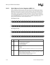
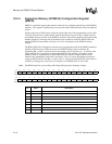
10.2.2 DRAM CAS Waveform Shift Registers (MDCAS0, MDCAS1,
MDCAS2)
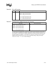
MDCAS0, MDCAS1, and MDCAS2 are 32-bit read/write registers that contain the nCAS
waveform for a full 8-beat burst read or write to asynchronous DRAM. Each bit represents one
CPU cycle if MDCNFG:CDB2 is 0 and 2 CPU cycles (1 memory clock cycle) if MDCNFG:CDB2
is 1. The least significant bit of MDCAS0 goes out first and is the cycle coincident with the
assertion of nRAS. Bit 1 is one cycle after the assertion of nRAS, and so on. MDCAS1 is
appended after MDCAS0 and MDCAS2 is appended after MDCAS1. A 1 in any field causes
nCAS to be deasserted in that cycle; a 0 causes nCAS to be asserted in that cycle. The memory
controller counts nCAS pulses and deasserts nRAS in the cycle following the deassertion of the
final nCAS pulse of the burst. All eight nCAS pulses must be programmed or the processor will
hang. When MDCNFG:CDB2 is 0, the MDCAS0 must contain 1s in the lower 4 bits and each
transition of nCAS must be a minimum of 2 clocks (nCAS must be asserted for a minimum of
2 CPU clock cycles and deasserted for 2). When MDCNFG:CDB2 is 1, the MDCAS0 must contain
1s in the lower 2 bits and each transition of nCAS must be a minimum of 1 bit. These registers are
unaffected by reset.


