SA-1100 Developer’s Manual 10-11
Memory and PCMCIA Control Module
1
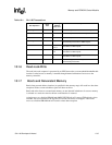
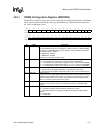
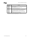
When SMCNFGx:RT=01, accesses to the selected bank will output a byte mask on nCAS<3:0> for both reads and writes. This
option should be selected only when there is no DRAM in the system.
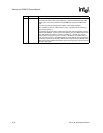
12..8 RDNx<4:0> ROM delay next access.
Number of memory clock cycles (minus 1) from address to data valid for subsequent
accesses of a burst ROM.
For Flash and SRAM, this determines the write pulse width.
One memory clock cycle is added to this value.
15..13 RRRx<2:0> ROM/SRAM recovery time.
Number of memory clock cycles (divided by 2) from chip select deasserted after a
read to next chip select (of a different memory bank) or nRAS asserted. nCS
negated to nRAS asserted is 2*RRR or 1 cycle (whichever is greater).
For Flash and SRAM, this field will also be used after writes to hold off subsequent
accesses.
This field should be programmed with the maximum of Toff, write pulse high time
(Flash/SRAM), and write recovery before read (Flash).
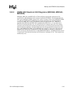
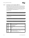
Bit Name Description


