SA-1100 Developer’s Manual 11-87
Peripheral Control Module
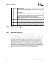
11.9.3.7 Receive Clock Edge Select (RCE)
When sample clock operation is enabled (SCE=1), the receive clock edge select (RCE) bit is used
to select which edge of the clock input from or output to GPIO pin 16 to use (rising or falling) to
synchronously sample data from the receive pin. When RCE=0, each bit received is sampled on the
rising edge of the sample clock; when RCE=1, bits are sampled on the clock’s falling edge. Note
that the internal baud rate generator and receive logic’s digital PLL are not used in this mode.
11.9.3.8 Transmit Clock Edge Select (TCE)
When sample clock operation is enabled (SCE=1), the transmit clock edge select (TCE) bit is used
to select which edge of the clock input from or output to GPIO pin 16 to use (rising or falling) to
synchronously drive data onto the transmit pin. When TCE=0, each bit transmitted is driven on the
rising edge of the sample clock; when TCE=1, bits are driven on the clock’s falling edge. Note that
the internal baud rate generator is not used in this mode.
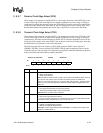
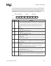
The following table shows the location of all bit fields located in SDLC control register 0
(SDCR0). The SDLC must be disabled (SUS=RXE=TXE=0) when changing the state of any bit
within this register. The reset state of all control bits except SUS is unknown (indicated by question
marks) and must be initialized before enabling the SDLC.
.
Address: 0h 8002 0060 SDCR0 Read/Write
Bit 7 6 5 4 3 2 1 0
TCE RCE SCD SCE BMS LBM SDF SUS
Reset ? ? ? ? ? ? ? 0
Bit Name Description
0SUS
SDLC/UART select.
0 – SDLC mode selected.
1 – UART mode selected.
Note: For SUS=0, if TXE=0, TXD1 control is given to PPC unit; if RXE=0, RXD1 control is
given to PPC unit. If UPR is set in the PPC unit, SUS is ignored, the UART uses
GPIO<14> to transmit and GPIO<15> to receive data, and serial port 1 defaults to SDLC
mode. The user must also program the GAFR and GPDR registers appropriately in the
GPIO unit.
1SDF
Single/double flag select.
0 – One flag generated at start of each transmit frame.
1 – Two flags generated at start of each transmit frame.
Note: SDF does not affect receive operation.
2LBM
Loopback mode.
0 – Normal serial port operation enabled.
1 – Output of transmit serial shifter is connected to input of receive serial shifter internally
and control of TXD1 and RXD1 pins is given to the PPC unit.
3BMS
Bit modulation select.
0 – FM0 bit encoding/decoding selected.
1 – NRZ bit encoding/decoding selected.
Note: BMS must be programmed to select NRZ (BMS=1) encoding when sample clock
operation is enabled (SCE=1).


