10-20 SA-1100
Developer’s Manual
Memory and PCMCIA Control Module
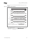
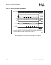
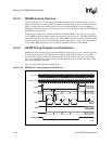
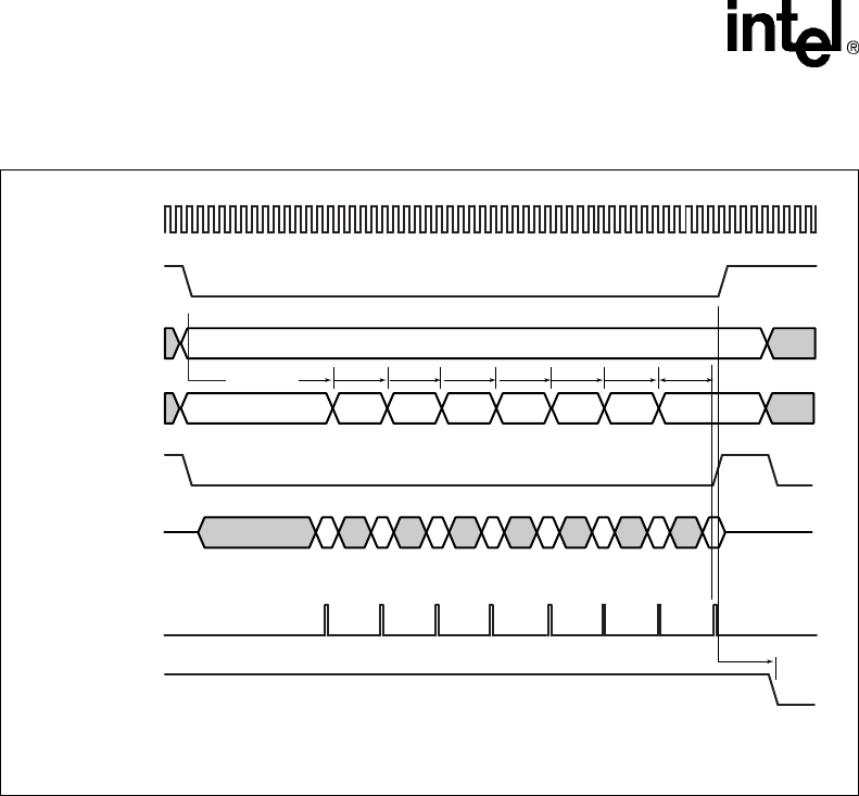
Figure 10-6. Burst-of-Eight ROM Timing Diagram
A4780-01
Memory Clock
Note: One extra CPU cycle (1/2 memory cycle) is added to the first access after nCS is asserted.
In this example, MSC0:SCNFG0:RDF = 12 (decimal), RDN = 4, RRR = 2.
nCS0
RDF+1.5
RDN+1 RDN+1 RDN+1 RDN+1 RDN+1 RDN+1 RDN+1
(2*RRR)+1
A[25:5]
A[4:2]
Input Data
Input Data
nCS1
Latch
nOE
0
D0 D1 D2 D4 D5
123456 7
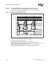
Note: One extra CPU cycle (1/2 memory cycle) is added to the first access after nCS is a
s
In this example, MSC0:SCNFG0:RDF=12(decimal), RDN=4, RRR=2.


