


10-10 SA-1100
Developer’s Manual
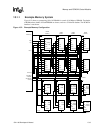
Memory and PCMCIA Control Module
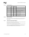
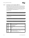
10.2.3 Static Memory Control Registers (MSC1–0)
MSC1 and MSC0 are read/write registers and contain control bits for configuring static memory
selected by nCS<3:0>. Reset forces the values in these registers to the slowest possible nonburst
ROM timing. Timing fields are specified as numbers of memory clock cycles. The memory clock
cycle consists of two CPU cycles. Each register contains two identical fields, for a total of four
identical fields, each corresponding to the chip select, nCS<x>, of the same number. On hardware
reset, the MSC0:SMCNFG0 field is set to 0b 1111 1111 1111 1x00 (binary) where x represents the
inverse of the ROM_SEL pin. All other fields in MSC0 and MSC1 are unaffected by reset;
question marks indicate that the values are unknown at reset.
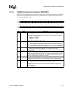
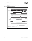
MSC0 Register Format
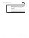
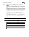
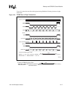
MSC1 Register Format
Bit31302928272625242322212019181716
Read RRR1_2 RRR1_1 RRR1_0 RDN1_4 RDN1_3 RDN1_2 RDN1_1 RDN1_0 RDF1_4 RDF1_3 RDF1_2 RDF1_1 RDF1_0 RBW1 RT1_1 RT1_0
Reset????????????????
-?
Bit1514131211109876543210
Read RRR0_2 RRR0_1 RRR0_0 RDN0_4 RDN0_3 RDN0_2 RDN0_1 RDN0_0 RDF0_4 RDF0_3 RDF0_2 RDF0_1 RDF0_0 RBW0 RT0_1 RT0_0
Reset1111111111111x00
Bit31302928272625242322212019181716
Read RRR3_2 RRR3_1 RRR3_0 RDN3_4 RDN3_3 RDN3_2 RDN3_1 RDN3_0 RDF3_4 RDF3_3 RDF3_2 RDF3_1 RDF3_0 RBW3 RT3_1 RT3_0
Reset????????????????
-?
Bit1514131211109876543210
Read RRR2_2 RRR2_1 RRR2_0 RDN2_4 RDN2_3 RDN2_2 RDN2_1 RDN2_0 RDF2_4 RDF2_3 RDF2_2 RDF2_1 RDF2_0 RBW2 RT2_1 RT2_0
Reset????????????????
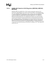
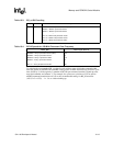
Bit Name Description
1..0 RTx<1:0> ROM type.
00 – Nonburst ROM or Flash EPROM.
01 – Nonburst ROM or SRAM.
1
10 – Burst-of-four ROM.
11 – Burst-of-eight ROM.
2 RBWx ROM bus width.
0 – 32 bits
1 – 16 bits
On reset, the RBW field in SMCNFG0 is loaded with the inverse of the ROM_SEL
pin.
7..3 RDFx<4:0> ROM delay first access.
Number of memory clock cycles (minus 1) from address to data valid for a nonburst
ROM or the first access of a burst ROM.
For Flash and SRAM, this determines the read access time.
One memory clock cycle is added to this value.