


SA-1100 Developer’s Manual 9-9
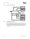
System Control Module
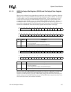
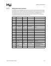
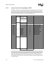
9.1.2 GPIO Alternate Functions
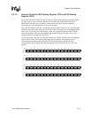
Most GPIO pins have an alternate function that can be invoked to enable additional functionality
within the SA-1100. If a GPIO is used for this alternate function, then it cannot be used as a GPIO
at the same time. Pins 0 and 1 are reserved because of their special use during sleep mode and are
not available for any alternate function. The following table shows each GPIO pin and its
corresponding alternate function. For more details on an alternate function, see the section that
corresponds to its name in the Unit column in the table.
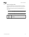
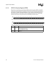
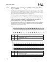
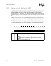
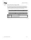
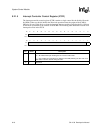
Pin Alternate Function Direction Unit Signal Description
GP<27> 32KHZ_OUT
Output Clocks Raw 32.768-kHz oscillator output
GP<26> RCLK_OUT
Output Clocks Internal clock/2
GP<25> RTC clock
Output RTC Trimmed 1-Hz clock
GP<24> Reserved
— — —
GP<23> TREQB
Input Test controller TIC request B
GP<22> TREQA/MBREQ
Input Test controller Either TIC request A or MBREQ
GP<21> TIC_ACK/MBGNT
Output Test controller
Either TIC acknowledge or
MBGNT
GP<21> MCP_CLK
Input Serial port 4 MCP clock in
GP<20> UART_SCLK3
Input Serial port 3:UART Sample clock input
GP<19> SSP_CLK
Input Serial port 2:SSP Sample clock input
GP<18> UART_SCLK1
Input Serial port 1:UART Sample clock input
GP<17> SDLC_AAF
Output Serial port 1:SDLC Abort after frame control
GP<16> SDLC_SCLK
I/O Serial port 1:SDLC Geoport clock out
GP<15> UART_RXD
Input Serial port 1:UART UART receive
GP<14> UART_TXD
Output Serial port 1:UART UART transmit
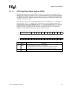
GP<13> SSP_SFRM
Output Serial Port 4:SSP SSP frame clock
GP<12> SSP_SCLK
Output Serial port 4:SSP SSP serial clock
GP<11> SSP_RXD
Input Serial port 4:SSP SSP receive
GP<10> SSP_TXD
Output Serial port 4:SSP SSP transmit
GP<2..9> LDD<8..15>
Output LCD controller
High-order data pins for
split-screen color LCD support
GP<1> Reserved
— — No alternate function
GP<0> Reserved
—- — No alternate function