10-12 SA-1100
Developer’s Manual
Memory and PCMCIA Control Module
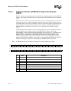
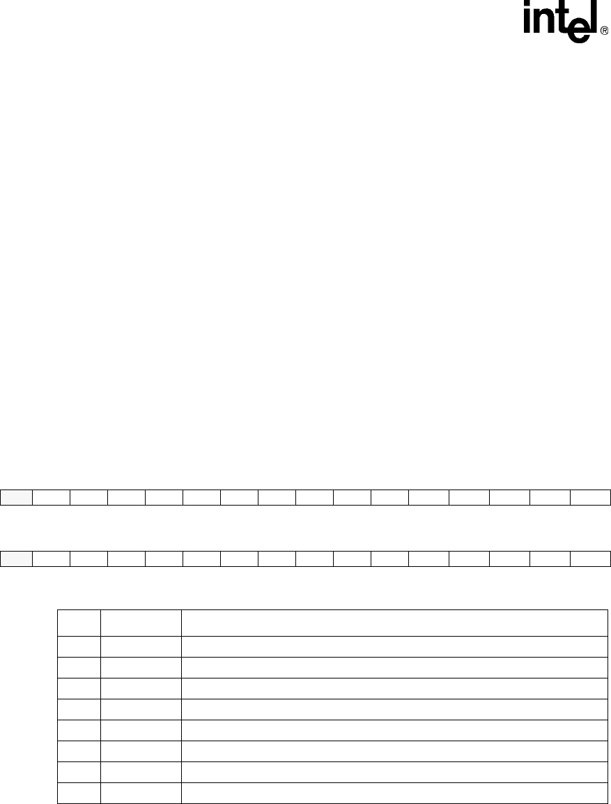
10.2.4 Expansion Memory (PCMCIA) Configuration Register
(MECR)
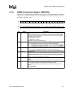
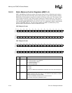
MECR is a read/write register that contains control bits for configuring the timing of the PCMCIA
interface. This register is unaffected by reset; question marks indicate that the values are unknown
at reset.
Writes to the reserved fields have no effect and reads return zeros. The programming of each of the
six fields allows the user to individually select the duration of accesses to I/O, common memory,
and attribute memory for each of two PCMCIA card slots. Each field is identical and represents the
number of memory clocks per tick of an internal clock, referred to as BCLK. BCLK clocks the
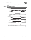
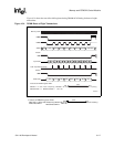
internal PCMCIA state machine. See Figure 10-15 for a description of the PCMCIA timing
diagram.
The BCLK_SEL field is designed to allow the user to program the speeds of the PCMCIA memory,
attribute, and I/O accesses. When an access to a PCMCIA address space is detected, the
appropriate BS_xx field is selected based on the memory map. Every (BS_xx + 1) memory clock
cycles, a BCLK tick is generated to advance the PCMCIA state machine. All signals (except
nPWAIT, which is asynchronous) on the PCMCIA bus are driven or sampled relative to this
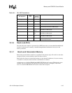
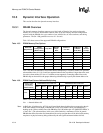
internal clock, although the clock itself is not driven. Table 10-3 shows the number of processor
clocks per BCLK tick for each BS_xx value. Table 10-4 shows the internal BCLK cycle times for
each BS_xx setting given a processor core frequency of 160 MHz (6.25-ns cycle time).
Note: The BCLK speed for a given setting will change if the processor frequency changes.
Bit313029282726252423222120 19 18 17 16
Read RES BSM2_4 BSM2_3 BSM2_2 BSM2_1 BSN2_0 BSA2_4 BSA2_3 BSA2_2 BSA2_1 BSA2_0 BSIO2_4 BSIO2_3 BSIO2_2 BSIO2_1 BSIO2_0
Reset???????????? ? ? ? ?
-?
Bit151413121110987654 3 2 1 0
Read RES BSM1_4 BSM1_3 BSM1_2 BSM1_1 BSN1_0 BSA1_4 BSA1_3 BSA1_2 BSA1_1 BSA1_0 BSIO1_4 BSIO1_3 BSIO1_2 BSIO1_1 BSIO1_0
Reset???????????? ? ? ? ?
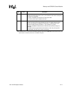
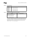
Bit Name Description
4..0 BSIO1<4:0> Clock count for accesses to PCMCIA card slot 1, I/O space.
9..5 BSA1<4:0> Clock count for accesses to PCMCIA card slot 1, attribute space.
14..10 BSM1<4:0> Clock count for accesses to PCMCIA card slot 1, common memory space.
15 — Reserved.
20..16 BSIO2<4:0> Clock count for accesses to PCMCIA card slot 2, I/O space.
25..21 BSA2<4:0> Clock count for accesses to PCMCIA card slot 2, attribute space.
30..26 BSM2<4:0> Clock count for accesses to PCMCIA card slot 2, common memory space.
31 — Reserved.


