


CPLD: Boot and Reset Registers
KAT4000 User’s Manual 10007175-02
7-8
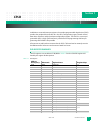
FWP1: Flash 1 Write Protect
1 Not write protected
0Write protected
FWP0: Flash 0 Write Protect
1 Not write protected
0Write protected
NFWP: NAND Flash Write Protect
1Write protected
0 Not write protected
SDA: I
2
C SDA Output Driver State
Bit state indicates PLD’s output level on the bus
SCL: I
2
C SCL Output Driver State
Bit state indicates PLD’s output level on the bus
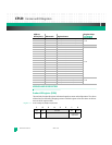
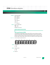
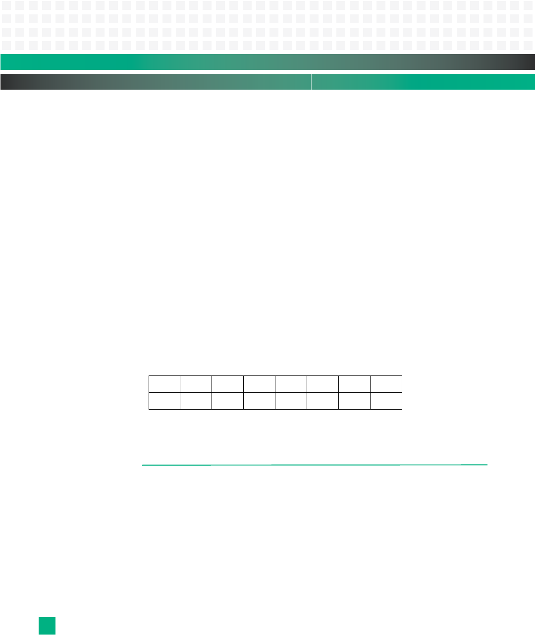
Scratch Register 1 (SCR1)
Scratch register 1 can be used as a reading/writing test register. Default register values are
shown in the bottom row of the register table.
Register 7-11: Scratch Register 1 (SCR1) at 0xfc40,002c
SCR7-0: Scratch bits
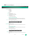
BOOT AND RESET REGISTERS
The reset signals are routed to and distributed by the CPLD. To support this functionality,
the CPLD includes three registers: one indicates the reason for the last reset, and the other
two force one of several types of reset.
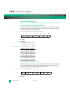
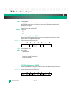
Reset Event Register (RER)
The read-only Reset Event register contains the bit corresponding to the most recent event
which caused a reset. If the entire register does not contain a bit (1), it is a Power On Reset
(POR) condition. Default register values are dependent on reset events.
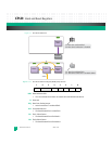
76543210
SCR7 SCR6 SCR5 SCR4 SCR3 SCR2 SCR1 SCR0
00000000