10007175-02 KAT4000 User’s Manual
10-1
Section 10
Synchronization Clocks
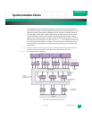
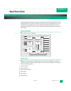
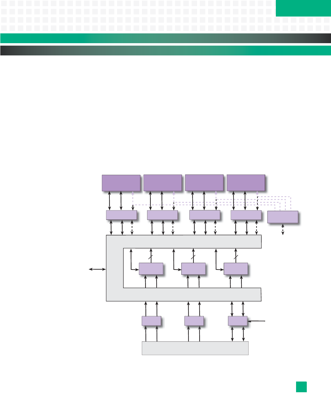
The KAT4000 implements a flexible clocking circuit based on a clock selection/holdover
chip with a PLD wrapper. This PLD wrapper allows local software control of the source clock
selection from these input options: backplane CLK1A/B, backplane CLK2A/B, backplane
CLK3A/B, AMCn TCLKA, AMCn TCLKB or AMCn FCLKA. Any of these clock sources can be
sent to the following output clocks: backplane CLK3A/B, AMCn TCLKA, AMCn TCLKB or
AMCn FCLKA. Transceiver buffers are used to convert all M-LVDS clocks to/from TTL levels.
CLK1 and CLK2 on the backplane are inputs only. See
Fig. 10-1 for a diagram of this circuitry.
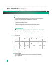
See “Clock Synchronizer Registers” on page 7-13 for information on configuring the stra-
tum clock buffers, selecting the primary and secondary clock sources, and selecting the
output source.
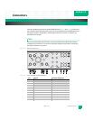
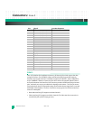
Note: The pins for TCLKC and TCLKD are routed to the Zone 3 connector interface. If these signals are used on a
rear transition module, there could be a conflict with an AMC module that uses these clocks.
Figure 10-1: Synchronization Clock Circuit Diagram
Clock
Transceiver
AMC 1
AMC 2
AMC 3
AMC 4
Clock
Selection 1
Clock
Selection 2
Clock
Selection 3
PLD Wrapper
Processor
Interface
via Local Bus
PCIe Clock
Source
Clock
Transceiver
Clock
Transceiver
Clock
Transceiver
E-key Enable
from Processor
Clock
Transceiver
Clock
Transceiver
Clock
Transceiver
PCIe REFCLK
Distribution
* FCLKA is either a PCIe REFCLK or standard clock signal.
Three Frequency
Output Paths:
19.44 MHz
1.54 MHz
2.048 MHz
Primary and Secondary
Clock Inputs
ATCA J20


