


Central Processing Unit: Microprocessor Core (e500)
KAT4000 User’s Manual 10007175-02
3-6
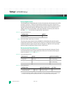
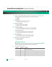
L2LFR: L2 cache Lock bits Flash Reset—L2 cache must be enabled for reset to occur (reserved in full
memory-mapped SRAM mode).
0 L2 cache lock bits are not cleared or the clear operation completed
1 Reset operation clears each L2 cache line’s lock bits
L2LFRID: L2 cache Lock bits Flash Reset select Instruction or Data—indicates whether data, instruc-
tion, or both bits are reset.
00 Not used
01 Reset data locks if L2LFR=1
10 Reset instruction locks if L2LFR=1
11 Reset both data and instruction locks if L2LFR=1
L2STASHDIS: L2 Stash allocate Disable—disables allocation of lines for stashing.
00 L2 allocates lines
01 L2 does not allocate lines
L2STASH: L2 Stash configuration—reserves regions of cache for stash-only operation.
00 No stash-only region
01 One-half of the array is stash-only
10 One-quarter of the array is stash-only
11 One-eighth of the array is stash-only
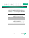
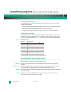
Hardware Implementation Dependent 0 Register
The Hardware Implementation Dependent 0 (HID0) register contains bits for
CPU-specific features. Most of these bits are cleared on initial power-up of the KAT4000.
Please refer to the MPC8548 PowerQuicc III Integrated Communications Processor Reference
Manual for more detailed descriptions of the HIDx registers. The following register map
summarizes HID0 for the MPC8548 processor:
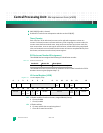
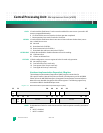
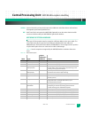
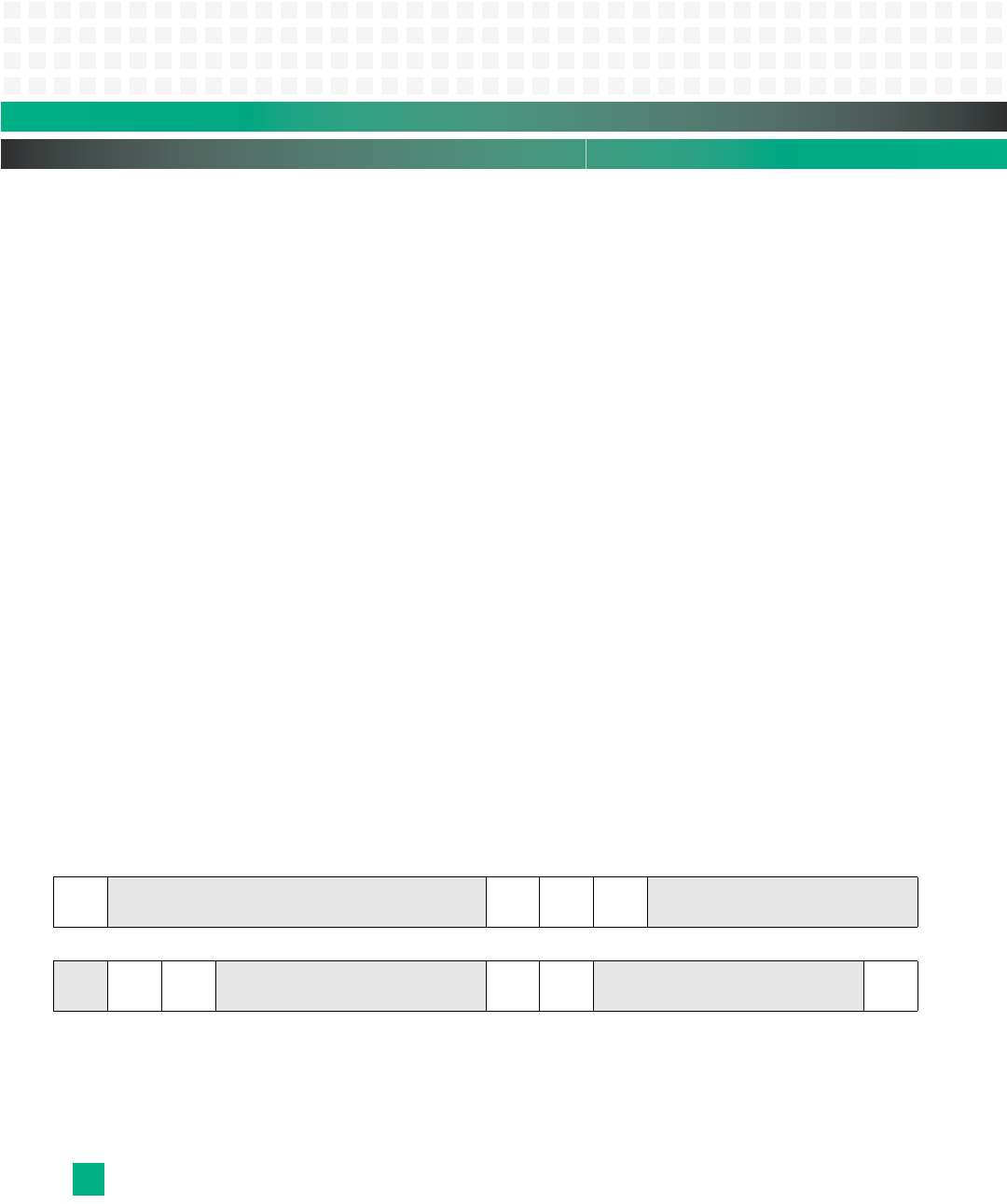
Register 3-2: MPC8548 Hardware Implementation Dependent Register 0 (HID0)
EMCP: Enable Machine Check Pin—masks further machine check exceptions caused by assertion of
MCP*.
0 MCP* is disabled
1 MCP* is enabled
32 33 39 40 41 42 43 47
EM
CP
reserved DOZ
E
NAP SLP reserved
48 49 50 51 55 56 57 58 62 63
RTB
EN
STB
CLK
reserved
EN_
MAS7
DCF
A
reserved NOP
TI