Central Processing Unit: MPC8548 Functions
10007175-02 KAT4000 User’s Manual
3-3
MPC8548 FUNCTIONS
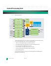
The MPC8548 provides the following functions on the KAT4000 module.
•Dual UART devices
•Two I
2
C controllers
• Programmable interrupt controller
•DDR2 SDRAM memory controller
• General-purpose I/O (GPIO)
• Chip select generation for the local bus devices
• DMA capability
•PCI-X bus interface
•sRIO or PCIe controller
• Four three-speed Ethernet controllers
MICROPROCESSOR CORE (E500)
L1 Cache
The MPC8548 processor implements two separate 32-kilobyte, level-one (L1) instruction
and data caches that are eight-way, set-associative. The L1 supports a four-state modi-
fied/exclusive/shared/invalid (MESI) cache coherency protocol. The caches also employ
pseudo-least recently used (PLRU) replacement algorithms within each way.
L2 Cache
The internal 512 kilobyte L2 cache is an eight-way set associative instruction and data
cache. The L2 cache is fully pipelined to provide 32 bytes per clock to the L1 caches. The L2
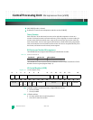
Control (L2CTL) register configures and operates the L2 SRAM array. The L2CTL is
read/write and contents are cleared during power-on reset.
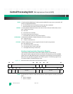
The L2 cache is cleared following a power-on or hard reset. Before enabling the L2 cache,
configuration parameters must be set in the L2CR and the L2 tags must be globally invali-
dated. Initialize the L2 cache during system start-up per the following sequence:
1 Power-on reset is automatically performed by the assertion of HRESET* signal.
2 Verify that L2CR[L2E] = 0.
3 Perform an L2 global invalidate by setting L2CR[L21].


