Central Processing Unit: JTAG/COP Interface
KAT4000 User’s Manual 10007175-02
3-14
JTAG/COP INTERFACE
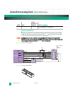
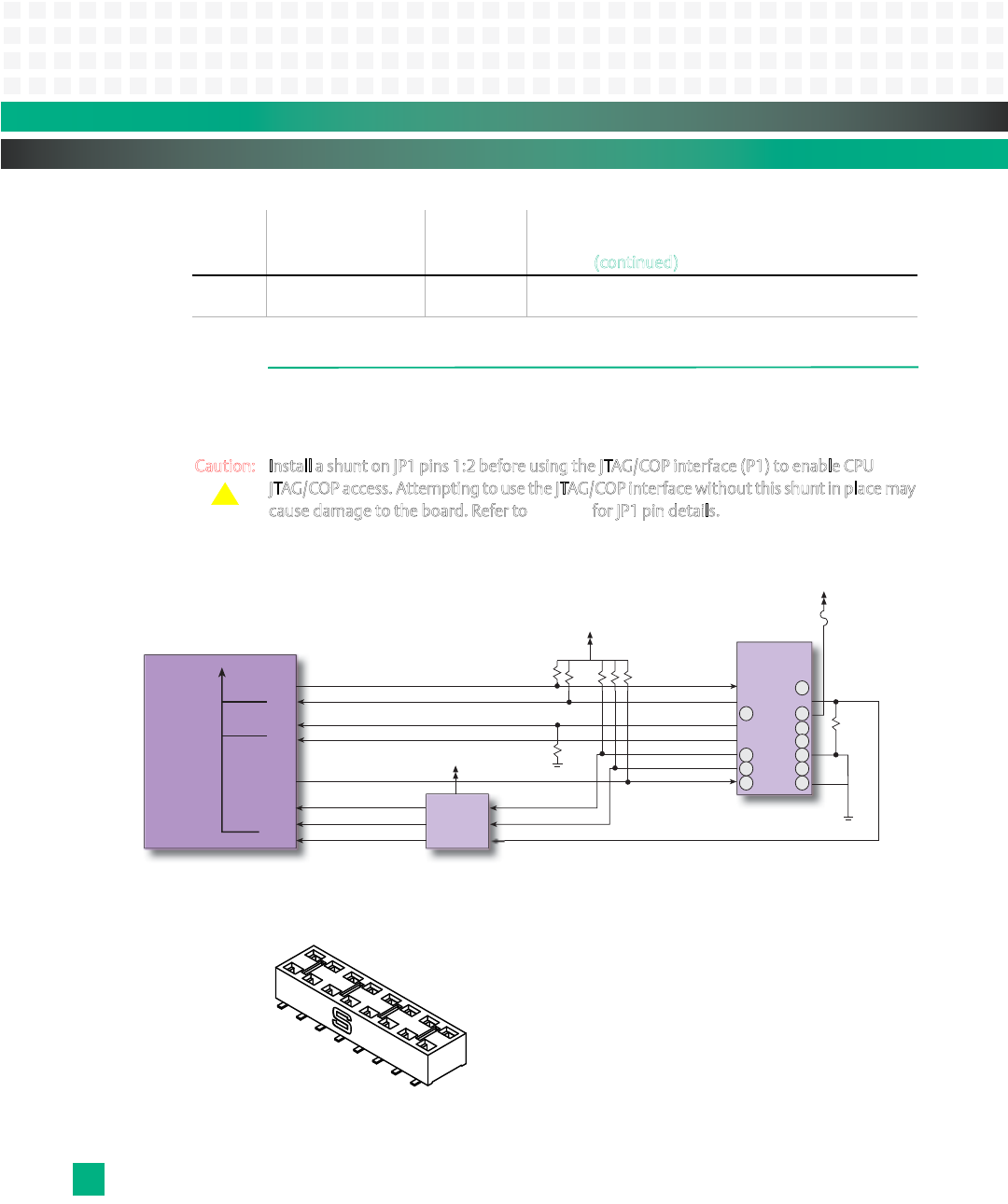
A single JTAG/COP header is provided for debug purposes for the processor. This interface
provides for boundary-scan testing of the CPU (see
Fig.3-2) and is compliant with the IEEE
1149.1 standard. The header pin assignments are defined in
Table 3-6.
C
aution: Install a shunt on JP1 pins 1:2 before using the JTAG/COP interface (P1) to enable CPU
J
TAG/COP access. Attempting to use the JTAG/COP interface without this shunt in place may
c
ause damage to the board. Refer to
Table 7-3 for JP1 pin details.
Figure 3-2: Processor JTAG/COP Diagram
Figure 3-3: Processor JTAG/COP Header
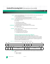
IVOR15 Debug 00F00 Caused when a debug exception exists in the DBSR and
when DBCR0[IDM]=1 and MSR[DE]=1
IVOR: Type:
Vector
Offset Hex
Address: Notes: (continued)
!
DEBUG_HRESET*
DEBUG_SRESET*
DEBUG_TRST*
COP
Debug
15
TDO
TDI
TCK
TMS
TRST*
16
2
3_3V (2.5V optional)
.75A
PICO_FUSE
MPC8548
Processor
Internal PU
TDO
TDI
TCK
TMS
CKSTP_OUT*
TRST*
KSL
PLD
3_3V
CPU_TDO
CPU_TDI
CPU_TCK
CPU_CKSTP_OUT*
CPU_TMS
CPU_HRESET*
CPU_SRESET*
CPU_TRST*
CPU_TDI
CPU_TCK
CPU_TMS
DEBUG_SRESET*
DEBUG_HRESET*
CPU_CKSTP_OUT*
CPU_TDO
3_3V
5.11K
5.11K
5.11K
5.11K


