


Page 96
Epson Research and Development
Vancouver Design Center
S1D13505 Hardware Functional Specification
X23A-A-001-14 Issue Date: 01/02/02
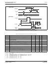
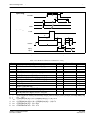
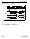
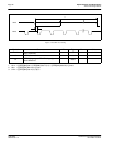
1. Ts = pixel clock period = memory clock, [memory clock]/2, [memory clock]/3, [memory clock]/4 (see REG[19h] bits [1:0])
2. t6
min
= [((REG[04h] bits [6:0])+1)*8 + ((REG[05h] bits [4:0])+1)*8] Ts
3. t7
min
= [((REG[07h] bits [3:0])+1)*8] Ts
4. t8
min
= [((REG[09h] bits [1:0], REG[08h] bits [7:0])+1) + ((REG[0Ah] bits [5:0])+1)] lines
5. t9
min
= [((REG[0Ch] bits [2:0])+1)] lines
6. t10
min
= [((REG[04h] bits [6:0])+1)*8] Ts
7. t12
min
= [((REG[06h] bits [4:0])*8)+1] Ts
8. t14
min
= [((REG[04h] bits [6:0])+1)*8] Ts
9. t15
min
= [((REG[06h] bits [4:0])+1)*8 - 2] Ts
10. t17
min
= [((REG[05h] bits [4:0])+1)*8 - ((REG[06h] bits [4:0])+1)*8 + 2]
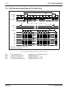
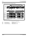
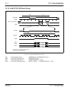
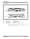
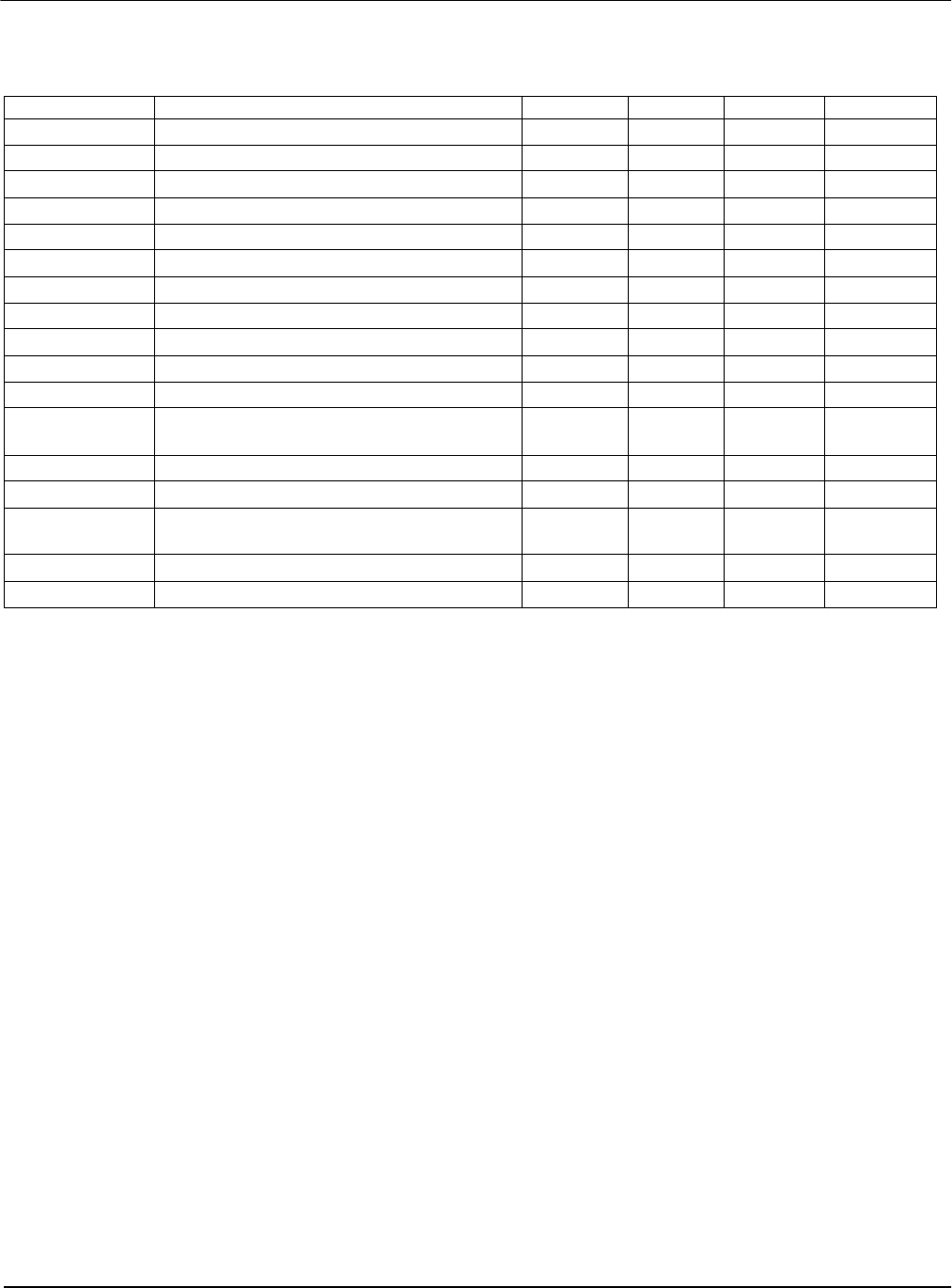
Table 7-32: TFT/D-TFD A.C. Timing
Symbol Parameter Min Typ Max Units
t1
FPSHIFT period
1 Ts (note 1)
t2
FPSHIFT pulse width high
0.45 Ts
t3
FPSHIFT pulse width low
0.45 Ts
t4
data setup to FPSHIFT falling edge
0.45 Ts
t5
data hold from FPSHIFT falling edge
0.45 Ts
t6
FPLINE cycle time
note 2
t7
FPLINE pulse width low
note 3
t8
FPFRAME cycle time
note 4
t9
FPFRAME pulse width low
note 5
t10
horizontal display period
note 6
t11
FPLINE setup to FPSHIFT falling edge
0.45 Ts
t12
FPFRAME pulse leading edge to FPLINE pulse
leading edge phase difference
note 7
t13
DRDY to FPSHIFT falling edge setup time
0.45 Ts
t14
DRDY pulse width
note 8
t15
DRDY falling edge to FPLINE pulse leading
edge
note 9
t16
DRDY hold from FPSHIFT falling edge
0.45 Ts
t17
FPLINE pulse leading edge to DRDY active
note 10 250 Ts