


Epson Research and Development
Page 117
Vancouver Design Center
Hardware Functional Specification S1D13505
Issue Date: 01/02/02 X23A-A-001-14
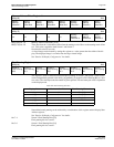
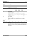
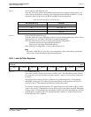
bit 6-5 CPU to Memory Wait State Bits [1:0]
These bits are used to optimize the handshaking between the host interface and the memory con-
troller. The bits should be set according to the relationship between BCLK and MCLK – see the
table below where T
B
and T
M
are the BCLK and MCLK periods respectively.
bits 4-0 Display FIFO Threshold Bits [4:0]
These bits specify the display FIFO depth required to sustain uninterrupted display fetches. When
these bits are all “0”, the display FIFO depth is calculated automatically.
These bits should always be set to 0, except in the following configurations:
Landscape mode at 15/16 bpp (with MCLK=PCLK),
Portrait mode at 8/16 bpp (with MCLK=PCLK).
When in the above configurations, a value of 1Bh should be used.
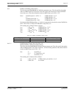
Note
The utility 13505CFG will, given the correct configuration values, automatically generate the
correct values for the Performance Enhancement Registers.
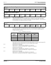
8.2.8 Look-Up Table Registers
bits 7-0 LUT Address Bits [7:0]
These 8 bits control a pointer into the Look-Up Tables (LUT). The S1D13505 has three 256-posi-
tion, 4-bit wide LUTs, one for each of red, green, and blue – refer to
“Look-Up Table Architecture”
for details.
This register selects which LUT entry is read/write accessible through the LUT Data Register
(REG[26h]). Writing the LUT Address Register automatically sets the pointer to the Red LUT.
Accesses to the LUT Data Register automatically increment the pointer.
For example, writing a value 03h into the LUT Address Register sets the pointer to R[3]. A subse-
quent access to the LUT Data Register accesses R[3] and moves the pointer onto G[3]. Subsequent
accesses to the LUT Data Register move the pointer onto B[3], R[4], G[4], B[4], R[5], etc. Note that
the RGB data is inserted into the LUT after the Blue data is written, i.e. all three colors must be
written before the LUT is updated.
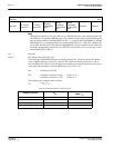
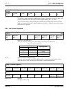
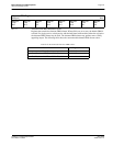
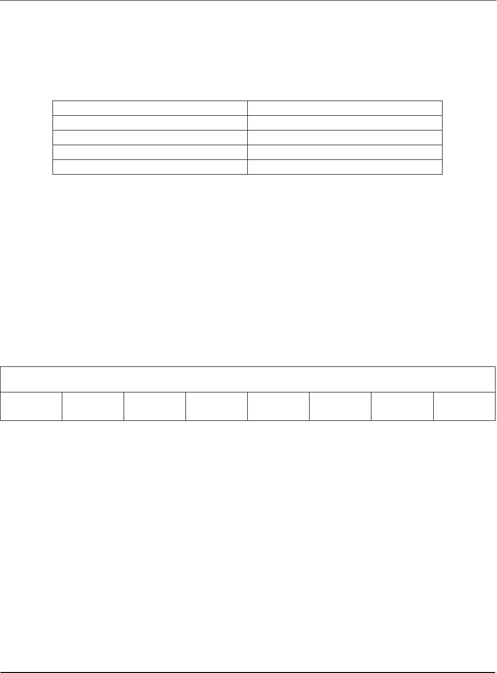
Table 8-16: Minimum Memory Timing Selection
Wait State Bits [1:0] Condition
00 no restrictions (default)
01 2T
M
- 4ns > T
B
10 undefined
11 undefined
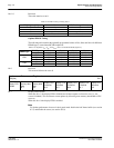
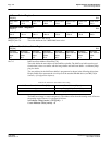
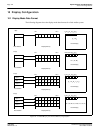
Look-Up Table Address Register
REG[24h] RW
LUT Address
Bit 7
LUT Address
Bit 6
LUT Address
Bit 5
LUT Address
Bit 4
LUT Address
Bit 3
LUT Address
Bit 2
LUT Address
Bit 1
LUT Address
Bit 0