


Page 32
Epson Research and Development
Vancouver Design Center
S1D13505 Hardware Functional Specification
X23A-A-001-14 Issue Date: 01/02/02
5.2.5 Miscellaneous
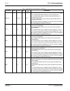
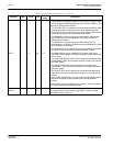
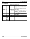
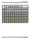
Table 5-4: Miscellaneous Interface Pin Descriptions
Pin Name Type Pin # Cell RESET# State Description
SUSPEND# IO 71 CS/TS1
Hi-Z if MD[9]=0
High if
MD[10:9]=01
Low if
MD[10:9]=11
This pin can be used as a power-down input (SUSPEND#)
or as an output possibly used for controlling the LCD
backlight power:
• When MD9 = 0 at rising edge of RESET#, this pin is an
active-low Schmitt input used to put the S1D13505 into
Hardware Suspend mode - see Section 15, “Power Save
Modes” for details.
• When MD[10:9] = 01 at rising edge of RESET#, this pin
is an output (GPO) with a reset state of 1. The state of GPO
is controlled by REG[21h] bit 7.
• When MD[10:9] = 11 at rising edge of RESET#, this pin
is an output (GPO) with a reset state of 0. The state of GPO
is controlled by REG[21h] bit 7.
CLKI I 69 C
Input clock for the internal pixel clock (PCLK) and memory
clock (MCLK). PCLK and MCLK are derived from CLKI - see
REG[19h] for details.
TESTEN I 70 CD Hi-Z
Test Enable. This pin should be connected to V
SS
for normal
operation.
VDD P
12, 33, 55, 72,
97, 109
PV
DD
DACVDD P 99, 102, 104 P DAC V
DD
VSS P
14, 32, 50, 68,
78, 87, 96, 110
PV
SS
DACVSS P 98, 106 P DAC V
SS