


Page 116
Epson Research and Development
Vancouver Design Center
S1D13505 Hardware Functional Specification
X23A-A-001-14 Issue Date: 01/02/02
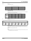
bits 1-0 Reserved
These bits must be set to 0.
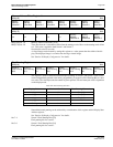
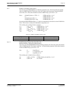
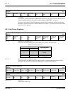
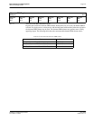
Optimal DRAM Timing
The following table contains the optimally programmed values of N
RC
, N
RP
, and N
RCD
for different
DRAM types, at maximum MCLK frequencies.
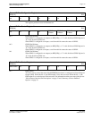
bit 0 Reserved
This reserved bit must be set to 0.
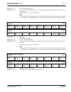
bit 7 Display FIFO Disable
When this bit = 1 the display FIFO is disabled and all data outputs are forced to zero (i.e., the
screen is blanked). This accelerates screen updates by allocating more memory bandwidth to CPU
accesses.
When this bit = 0 the display FIFO is enabled.
Note
For further performance increase in dual panel mode disable the half frame buffer (see section
8.2.7) and disable the cursor (see section 8.2.9).
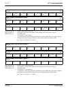
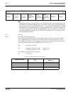
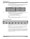
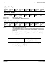
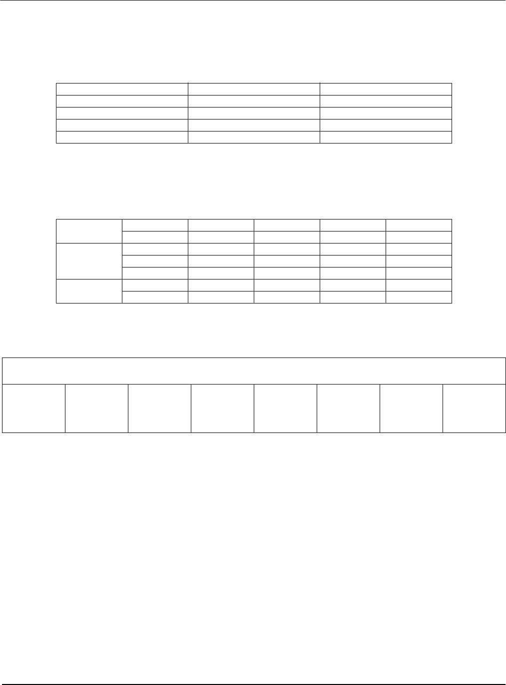
Table 8-14: RAS Precharge Timing Select
REG[22h] bits [3:2] N
RP
RAS# Precharge Width (t
RP
)
00 2 2
01 1.5 1.5
10 1 1
11 Reserved Reserved
Table 8-15: Optimal N
RC
, N
RP
, and N
RCD
values at maximum MCLK frequency
DRAM Type
DRAM Speed T
M
N
RC
N
RP
N
RCD
(ns) (ns) (#MCLK) (#MCLK) (#MCLK)
EDO
50 25 4 1.5 2
60 30 4 1.5 2
70 33 5 2 2
FPM
60 40 4 1.5 2
70 50 3 1.5 1
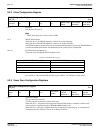
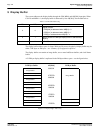
Performance Enhancement Register 1
REG[23h] RW
Display FIFO
Disable
CPU to
Memory Wait
State
Bit 1
CPU to
Memory Wait
State
Bit 0
Display FIFO
Threshold
Bit 4
Display FIFO
Threshold
Bit 3
Display FIFO
Threshold
Bit 2
Display FIFO
Threshold
Bit 1
Display FIFO
Threshold
Bit 0