


Page 100
Epson Research and Development
Vancouver Design Center
S1D13505 Hardware Functional Specification
X23A-A-001-14 Issue Date: 01/02/02
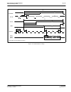
8.2.2 Memory Configuration Registers
bits 6-4 DRAM Refresh Rate Select Bits [2:0]
These bits specify the divisor used to generate the DRAM refresh rate from the input clock (CLKI).
bit 2 WE# Control
When this bit = 1, 2-WE# DRAM is selected.
When this bit = 0, 2-CAS# DRAM is selected.
bit 0 Memory Type
When this bit = 1, FPM-DRAM is selected.
When this bit = 0, EDO-DRAM is selected.
This bit should be changed only when there are no read/write DRAM cycles. This condition occurs
when all of the following are true: the Display FIFO is disabled (REG[23h] bit 7 = 1), and the Half
Frame Buffer is disabled (REG[1Bh] bit 0 = 1), and the Ink/Cursor is inactive
(Reg[27h] bits 7-6 = 00). This condition also occurs when the CRT and LCD enable bits (Reg[0Dh]
bits 1-0) have remained 0 since chip reset. For further programming information, see
S1D13505
Programming Notes and Examples
, document number X23A-G-003-xx.
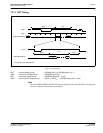
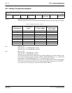
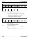
Memory Configuration Register
REG[01h] RW
n/a
Refresh Rate
Bit 2
Refresh Rate
Bit 1
Refresh Rate
Bit 0
n/a WE# Control n/a Memory Type
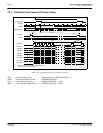
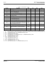
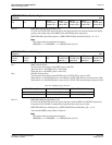
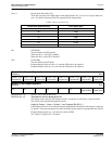
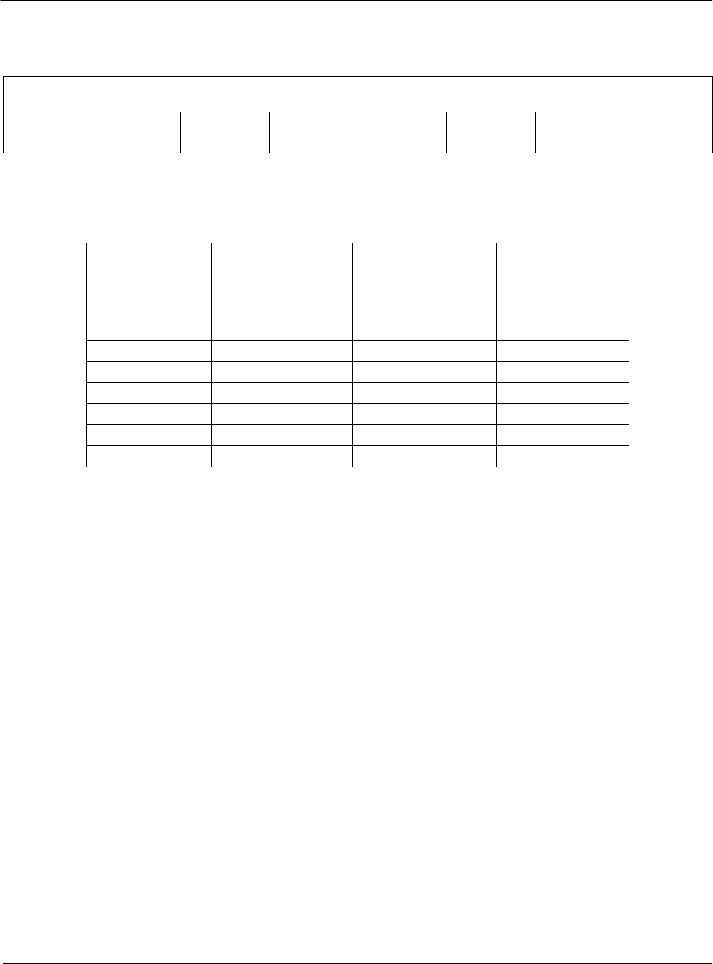
Table 8-2: DRAM Refresh Rate Selection
DRAM Refresh Rate
Select Bits [2:0]
CLKI Frequency
Divisor
Example Refresh Rate
for CLKI = 33MHz
Example period for
256 refresh cycles at
CLKI = 33MHz
000 64 520 kHz 0.5 ms
001 128 260 kHz 1 ms
010 256 130 kHz 2 ms
011 512 65 kHz 4 ms
100 1024 33 kHz 8 ms
101 2048 16 kHz 16 ms
110 4096 8 kHz 32 ms
111 8192 4 kHz 64 ms