


Page 114
Epson Research and Development
Vancouver Design Center
S1D13505 Hardware Functional Specification
X23A-A-001-14 Issue Date: 01/02/02
Note
Changing this register to non-zero value, or to a different non-zero value, should be done only
when there are no read/write DRAM cycles. This condition occurs when all of the following are
true: the Display FIFO is disabled (REG[23h] bit 7 = 1), and the Half Frame Buffer is disabled
(REG[1Bh] bit 0 = 1), and the Ink/Cursor is inactive (Reg[27h] bits 7-6 = 00). This condition also
occurs when the CRT and LCD enable bits (Reg[0Dh] bits 1-0) have remained 0 since chip reset.
For further programming information, see
S1D13505 Programming Notes and Examples
, docu-
ment number X23A-G-003-xx.
bit 7 Reserved
bits 6-5 RC Timing Value (N
RC
) Bits [1:0]
These bits select the DRAM random-cycle timing parameter, t
RC
. These bits specify the number
(N
RC
) of MCLK periods (T
M
) used to create t
RC
. N
RC
should be chosen to meet t
RC
as well as
t
RAS
, the RAS pulse width. Use the following two formulae to calculate N
RC
then choose the larger
value. Note, these formulae assume an MCLK duty cycle of 50 +/- 5%.
N
RC
= Round-Up (t
RC
/T
M
)
N
RC
= Round-Up (t
RAS
/T
M
+ N
RP
)if N
RP
= 1 or 2
= Round-Up (t
RAS
/T
M
+ 1.55) if N
RP
= 1.5
The resulting t
RC
is related to N
RC
as follows:
t
RC
= (N
RC
) T
M
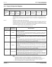
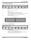
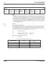
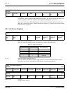
Performance Enhancement Register 0
REG[22h] RW
Reserved
RC Timing
Value Bit 1
RC Timing
Value Bit 0
RAS#-to-
CAS# Delay
Value
RAS#
Precharge
Timing Value
Bit 1
RAS#
Precharge
Timing Value
Bit 0
Reserved Reserved
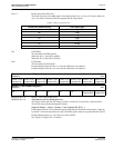
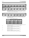
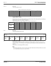
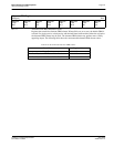
Table 8-12: Minimum Memory Timing Selection
REG[22h] bits [6:5] N
RC
Minimum Random Cycle
Width (
t
RC
)
00 5 5
01 4 4
10 3 3
11 Reserved Reserved