


Epson Research and Development
Page 27
Vancouver Design Center
Hardware Functional Specification S1D13505
Issue Date: 01/02/02 X23A-A-001-14
RD# I 7
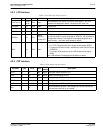
CS Hi-Z
This is a multi-purpose pin:
• For SH-3/SH-4 Bus, this pin inputs the read signal (RD#).
• For MC68K Bus 1, this pin is connected to V
DD
.
• For MC68K Bus 2, this pin inputs the bus size bit 1 (SIZ1).
• For Generic Bus, this pin inputs the read command for the lower data
byte (RD0#).
• For MIPS/ISA Bus, this pin inputs the memory read signal (MEMR#).
• For Philips PR31500/31700 Bus, this pin inputs the memory read
command (/RD).
• For Toshiba TX3912 Bus, this pin inputs the memory read command
(RD*).
• For PowerPC Bus, this pin inputs the transfer size 0 signal (TSIZ0).
• For PC Card (PCMCIA) Bus, this pin inputs the output enable signal
(-OE).
See
“Host Bus Interface Pin Mapping”
for summary. See the respective
AC Timing diagram for detailed functionality.
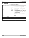
WE0# I 8
CS Hi-Z
This is a multi-purpose pin:
• For SH-3/SH-4 Bus, this pin inputs the write enable signal for the
lower data byte (WE0#).
• For MC68K Bus 1, this pin must be connected to V
DD
• For MC68K Bus 2, this pin inputs the bus size bit 0 (SIZ0).
• For Generic Bus, this pin inputs the write enable signal for the lower
data byte (WE0#).
• For MIPS/ISA Bus, this pin inputs the memory write signal
(MEMW#).
• For Philips PR31500/31700 Bus, this pin inputs the memory write
command (/WE).
• For Toshiba TX3912 Bus, this pin inputs the memory write command
(WE*).
• For PowerPC Bus, this pin inputs the Transfer Size 1 signal (TSIZ1).
• For PC Card (PCMCIA) Bus, this pin inputs the write enable signal (-
WE).
See
“Host Bus Interface Pin Mapping”
for summary. See the respective
AC Timing diagram for detailed functionality.
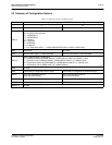
Table 5-1: Host Interface Pin Descriptions (Continued)
Pin Name Type Pin # Cell
RESET#
State
Description