


Epson Research and Development
Page 23
Vancouver Design Center
Hardware Functional Specification S1D13505
Issue Date: 01/02/02 X23A-A-001-14
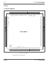
5.2 Pin Description
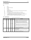
Key:
5.2.1 Host Interface
I = Input
O=Output
IO = Bi-Directional (Input/Output)
A=Analog
P=Power pin
C = CMOS level input
CD = CMOS level input with pull down resistor (typical values of 100K
Ω/180ΚΩ
at 5V/3.3V respectively)
CS = CMOS level Schmitt input
COx = CMOS output driver, x denotes driver type (see tables 6-3, 6-4, 6-5 for details)
TSx = Tri-state CMOS output driver, x denotes driver type (see tables 6-3, 6-4, 6-5 for details)
TSxD =
Tri-state CMOS output driver with pull down resistor (typical values of 100K
Ω/180ΚΩ
at 5V/3.3V)
respectively), x denotes driver type (see tables 6-3, 6-4, 6-5 for details)
CNx = CMOS low-noise output driver, x denotes driver type (see tables 6-3, 6-4, 6-5 for details)
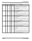
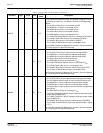
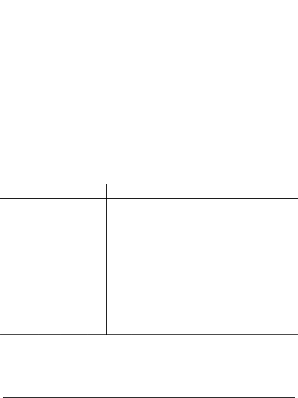
Table 5-1: Host Interface Pin Descriptions
Pin Name Type Pin # Cell
RESET#
State
Description
AB0 I 3
CS Hi-Z
• For SH-3/SH-4 Bus, this pin inputs system address bit 0 (A0).
• For MC68K Bus 1, this pin inputs the lower data strobe (LDS#).
• For MC68K Bus 2, this pin inputs system address bit 0 (A0).
• For Generic Bus, this pin inputs system address bit 0 (A0).
• For MIPS/ISA Bus, this pin inputs system address bit 0 (SA0).
• For Philips PR31500/31700 Bus, this pin inputs system address bit 0
(A0).
• For Toshiba TX3912 Bus, this pin inputs system address bit 0 (A0).
• For PowerPC Bus, this pin inputs system address bit 31 (A31).
• For PC Card (PCMCIA) Bus, this pin inputs system address bit 0
(A0).
See
“Host Bus Interface Pin Mapping”
for summary. See the respective
AC Timing diagram for detailed functionality.
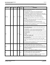
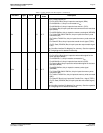
AB[12:1] I
119-128,
1, 2
CHi-Z
• For PowerPC Bus, these pins input the system address bits 19
through 30 (A[19:30]).
• For all other busses, these pins input the system address bits 12
through 1 (A[12:1]).
See
“Host Bus Interface Pin Mapping”
for summary. See the respective
AC Timing diagram for detailed functionality.