


Page 36
Epson Research and Development
Vancouver Design Center
S1D13505 Programming Notes and Examples
X23A-G-003-07 Issue Date: 01/02/05
These two registers form a value known as the line compare. When the line compare value
is equal to or greater than the physical number of lines being displayed there is no visible
effect on the display. When the line compare value is less than the number of physically
displayed lines, display operation works like this:
1. From the end of vertical non-display to the number of lines indicated by line compare
the display data will be from the memory pointed to by the Screen 1 Display Start Ad-
dress.
2. After
line compare
lines have been displayed the display will begin showing data
from Screen 2 Display Start Address memory.
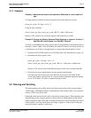
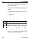
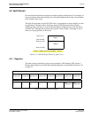
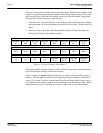
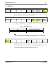
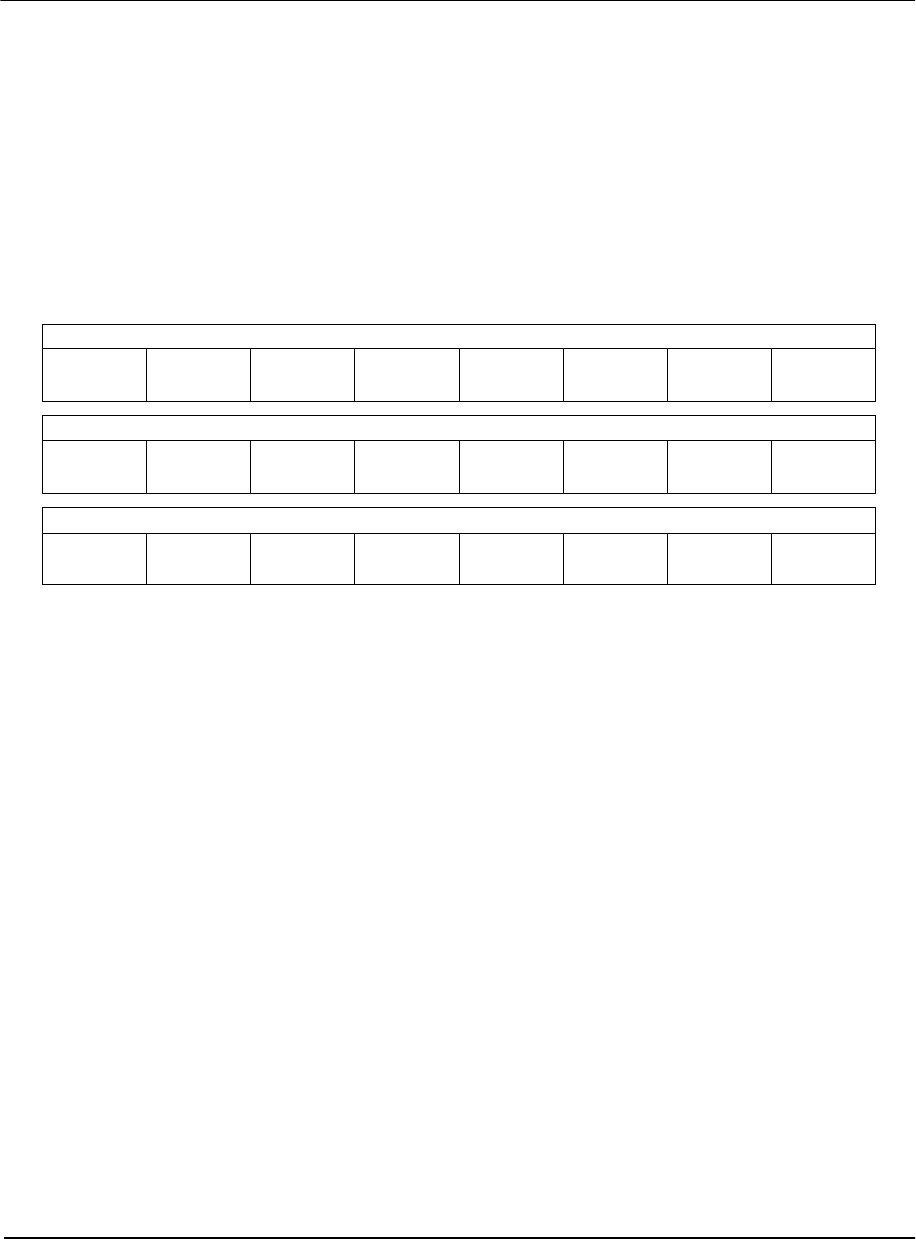
Figure 5-7: Screen 2 Display Start Address
These three registers form the twenty bit offset to the first word in the display buffer that
will be shown in the screen 2 portion of the display.
Screen 1 memory is
always
displayed first at the top of the screen followed by screen 2
memory. The start address for the screen 2 image may be lower in memory than that of
screen 1 (i.e. screen 2 could be coming from offset 0 in the display buffer while screen 1
was coming from an offset located several thousand bytes into the display buffer). While
not particularly useful, it is possible to set screen 1 and screen 2 to the same address.
REG[13h] Screen 2 Display Start Address Register 0
Start Addr
Bit 7
Start Addr
Bit 6
Start Addr
Bit 5
Start Addr
Bit 4
Start Addr
Bit 3
Start Addr
Bit 2
Start Addr
Bit 1
Start Addr
Bit 0
REG[14h] Screen 2 Display Start Address Register 1
Start Addr
Bit 15
Start Addr
Bit 14
Start Addr
Bit 13
Start Addr
Bit 12
Start Addr
Bit 11
Start Addr
Bit 10
Start Addr
Bit 9
Start Addr
Bit 8
REG[15h] Screen 2 Display Start Address Register 2
n/a n/a n/a n/a
Start Addr
Bit 19
Start Addr
Bit 18
Start Addr
Bit 17
Start Addr
Bit 16