


Epson Research and Development
Page 13
Vancouver Design Center
Programming Notes and Examples S1D13505
Issue Date: 01/02/05 X23A-G-003-07
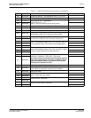
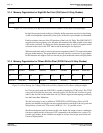
[06] 0000 0000 FPLINE start position - only required for CRT or TFT/D-TFD
[07] 0000 0000 FPLINE polarity set to active high
[08] 1110 1111 Vertical display size = Reg[09][08] + 1
= 0000 0000 1110 1111 + 1
= 239+1 = 240 lines (total height/2 for dual panels)
[09] 0000 0000
[0A] 0011 1000 Vertical non-display size = Reg[0A] + 1 = 57 + 1 = 58 lines
[0B] 0000 0000 FPFRAME start position - only required for CRT or TFT/D-TFD
[0C] 0000 0000 FPFRAME polarity set to active high
[0D] 0000 1100
Display mode - hardware portrait mode disabled, 8 bpp and
LCD disabled, enable LCD in last step of this example.
[0E] 1111 1111
Line compare (Regs[0Eh] and[0Fh] set to maximum allowable
value. We can change this later if we want a split screen.
‘
[0F] 0000 0011
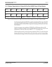
[10] 0000 0000
Screen 1 Start Address (Regs [10h], [11h], and [12h]) set to 0.
This will start the display in the first byte of the display buffer.
[11] 0000 0000
[12] 0000 0000
[13] 0000 0000
Screen 2 Start Address (Regs [13h], [14h], and [15h]) to offset
0. Screen 2 Start Address in not used at this time.
[14] 0000 0000
[15] 0000 0000
[16] 0100 0000 Memory Address Offset (Regs [17h] [16h])
- 640 pixels = 640 bytes = 320 words = 140h words
Note: When setting a horizontal resolution greater than 767
pixels, with a color depth of 15/16 bpp, the Memory Offset
Registers (REG[16h], REG[17h]) must be set to a virtual
horizontal pixel resolution of 1024.
[17] 0000 0001
[18] 0000 0000 Set pixel panning for both screens to 0
[19] 0000 0001
Clock Configuration - set PClk to MClk/2 - the specification says
that for a dual color panel the maximum PClk is MClk/2
[1A] 0000 0000 Enable LCD Power
[1C] 0000 0000
MD Configuration Readback - we write a 0 here to keep the
register configuration logic simpler
[1D] 0000 0000
[1E] 0000 0000
General I/O Pins - set to zero.
[1F] 0000 0000
[20] 0000 0000
General I/O Pins Control - set to zero.
[21] 0000 0000
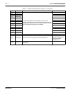
Table 2-1: S1D13505 Initialization Sequence (Continued)
Register Value Notes See Also