


Epson Research and Development
Page 9
Vancouver Design Center
Interfacing to the Motorola MPC821 Microprocessor S1D13505
Issue Date: 01/02/05 X23A-G-008-05
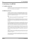
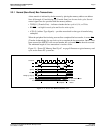
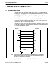
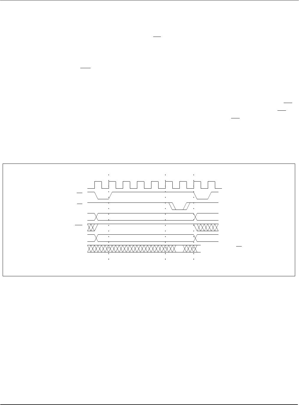
2.2.1 Normal (Non-Burst) Bus Transactions
A data transfer is initiated by the bus master by placing the memory address on address
lines A0 through A31 and driving TS
(Transfer Start) low for one clock cycle. Several
control signals are also provided with the memory address:
• TSIZ[0:1] (Transfer Size) -- indicates whether the bus cycle is 8, 16, or 32-bit.
• RD/WR
-- set high for read cycles and low for write cycles.
• AT[0:3] (Address Type Signals) -- provides more detail on the type of transfer being
attempted.
When the peripheral device being accessed has completed the bus transfer, it asserts TA
(Transfer Acknowledge) for one clock cycle to complete the bus transaction. Once TA
has
been asserted, the MPC821 will not start another bus cycle until TA
has been de-asserted.
The minimum length of a bus transaction is two bus clocks.
Figure 2-1: “Power PC Memory Read Cycle” on page 9 illustrates a typical memory read
cycle on the Power PC system bus.
Figure 2-1: Power PC Memory Read Cycle
A[0:31]
D[0:31]
TSIZ[0:1], AT[0:3]
TS
TA
SYSCLK
Wait StatesTransfer Start Transfer Next Transfer
Sampled when TA low
RD/WR
Complete Starts