


Epson Research and Development
Page 49
Vancouver Design Center
Hardware Functional Specification S1D13505
Issue Date: 01/02/02 X23A-A-001-14
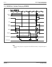
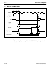
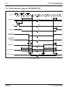
1. If the S1D13505 host interface is disabled, the timing for DSACK1# driven high is relative to
the falling edge of CS#, AS# or
the first positive edge of CLK after A[20:0], M/R# becomes
valid, whichever one is later.
2. If the S1D13505 host interface is disabled, the timing for D[31:16] driven is relative to the
falling edge of UDS#, LDS# or
the first positive edge of CLK after A[20:0], M/R# becomes
valid, whichever one is later.
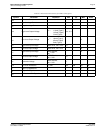
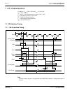
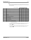
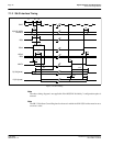
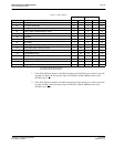
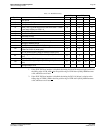
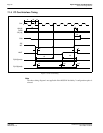
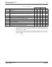
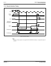
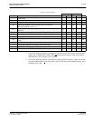
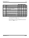
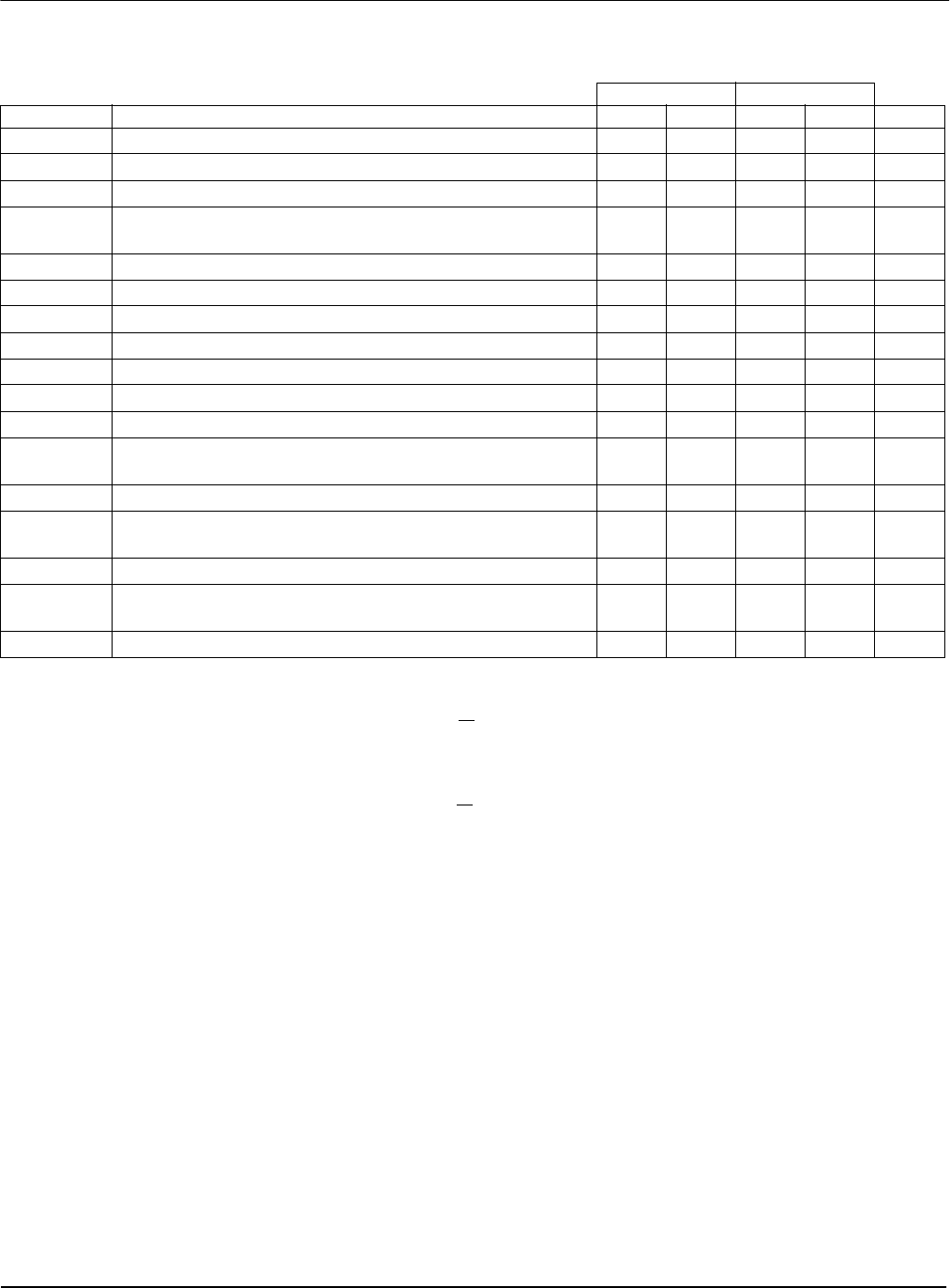
Table 7-4: MC68030 Timing
3.0V 5.0V
Symbol Parameter Min Max Min Max Units
t1
Clock period
20 20 ns
t2
Clock pulse width high
66ns
t3
Clock pulse width low
66ns
t4
A[20:0], SIZ[1:0], M/R# setup to first CLK where CS# = 0 AS# =
0, and either UDS#=0 or LDS# = 0
10 10 ns
t5
A[20:0], SIZ[1:0], M/R# hold from AS#
00ns
t6
CS# hold from AS#
00ns
t7
R/W# setup to DS#
10 10 ns
t8
R/W# hold from AS#
00ns
t9
1
AS# = 0 and CS# = 0 to DSACK1# driven high
00ns
t10
AS# high to DSACK1# high
318312ns
t11
First BCLK where AS# = 1 to DSACK1# high impedance
5 25 2.5 10 ns
t12
D[31:16] valid to third CLK where CS# = 0 AS# = 0, and either
UDS#=0 or LDS# = 0 (write cycle)
10 10 ns
t13
D[31:16] hold from falling edge of DSACK1# (write cycle)
00ns
t14
2
Falling edge of UDS#=0 or LDS# = 0 to D[31:16] driven (read
cycle)
00ns
t15
D[31:16] valid to DSACK1# falling edge (read cycle)
00ns
t16
UDS# and LDS# high to D[31:16] invalid/high impedance (read
cycle)
5 25 2.5 10 ns
t17
AS# high setup to CLK
22ns