


Epson Research and Development
Page 29
Vancouver Design Center
Hardware Functional Specification S1D13505
Issue Date: 01/02/02 X23A-A-001-14
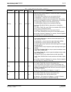
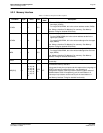
5.2.2 Memory Interface
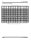
Table 5-2: Memory Interface Pin Descriptions
Pin Name Type Pin # Cell
RESET#
State
Description
LCAS# O 51 CO1 1
• For dual-CAS# DRAM, this is the column address strobe for the
lower byte (LCAS#).
• For single-CAS# DRAM, this is the column address strobe (CAS#).
See
“Memory Interface Pin Mapping”
for summary. See
Memory
Interface Timing
for detailed functionality.
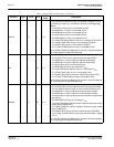
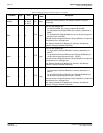
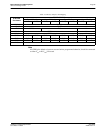
UCAS# O 52 CO1 1
This is a multi-purpose pin:
• For dual-CAS# DRAM, this is the column address strobe for the
upper byte (UCAS#).
• For single-CAS# DRAM, this is the write enable signal for the upper
byte (UWE#).
See
“Memory Interface Pin Mapping”
for summary. See
Memory
Interface Timing
for detailed functionality.
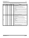
WE# O 53 CO1 1
• For dual-CAS# DRAM, this is the write enable signal (WE#).
• For single-CAS# DRAM, this is the write enable signal for the lower
byte (LWE#).
See
“Memory Interface Pin Mapping”
for summary. See
Memory
Interface Timing
for detailed functionality.
RAS# O 54 CO1 1
Row address strobe - see
Memory Interface Timing
for detailed
functionality.
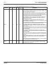
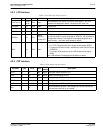
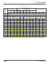
MD[15:0] IO
34, 36, 38,
40, 42, 44,
46, 48, 49,
47, 45, 43,
41, 39, 37,
35
C/TS
1D
Hi-Z
Bi-Directional memory data bus.
During reset, these pins are inputs and their states at the rising edge of
RESET# are used to configure the chip - see
Summary of
Configuration Options
. Internal pull-down resistors (typical values of
100K
Ω/180ΚΩ
at 5V/3.3V respectively) pull the reset states to 0.
External pull-up resistors can be used to pull the reset states to 1.
See
Memory Interface Timing
for detailed functionality.