


Epson Research and Development
Page 11
Vancouver Design Center
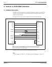
Interfacing to the NEC VR4121™ Microprocessor S1D13505
Issue Date: 01/02/05 X23A-G-011-04
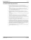
3.2 Host Bus Interface Signal Descriptions
The S1D13505 MIPS/ISA Host Bus Interface requires the following signals.
• BUSCLK is a clock input which is required by the S1D13505 Host Bus Interface. It is
separate from the input clock (CLKI) and is typically driven by the host CPU system
clock.
• The address inputs AB[20:0], and the data bus DB[15:0], connect directly to the
VR4121 address (ADD[20:0]) and data bus (DAT[15:0]), respectively. MD4 must be
set to select the proper endian mode upon reset.
• M/R# (memory/register) selects between memory or register access. It may be
connected to an address line, allowing system address ADD21 to be connected to the
M/R# line.
• Chip Select (CS#) must be driven low by LCDCS# whenever the S1D13505 is accessed
by the VR4121.
• WE1# connects to SHB# (the high byte enable signal from the VR4121) which in
conjunction with address bit 0 allows byte steering of read and write operations.
• WE0# connects to WR# (the write enable signal from the VR4121) and must be driven
low when the VR4121 bus is writing data to the S1D13505.
• RD# connects to RD# (the read enable signal from the VR4121) and must be driven low
when the VR4121 bus is reading data from the S1D13505.
• WAIT# connects to LCDRDY and is a signal output from the S1D13505 that indicates
the VR4121 bus must wait until data is ready (read cycle) or accepted (write cycle) on
the host bus. Since VR4121 bus accesses to the S1D13505 may occur asynchronously to
the display update, it is possible that contention may occur in accessing the S1D13505
internal registers and/or display buffer. The WAIT# line resolves these contentions by
forcing the host to wait until the resource arbitration is complete.
• The BS# and RD/WR# signals are not used for the MIPS/ISA Host Bus Interface and
should be tied high (connected to V
DD
).