


Epson Research and Development
Page 13
Vancouver Design Center
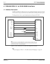
Interfacing to the NEC VR4102/VR4111™ Microprocessors S1D13505
Issue Date: 01/02/05 X23A-G-007-06
4.2 S1D13505 Hardware Configuration
The S1D13505 latches MD15 through MD0 to allow selection of the bus mode and other
configuration data on the rising edge of RESET#. For details on configuration, refer to the
S1D13505 Hardware Functional Specification, document number X23A-A-001-xx.
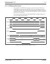
The table below shows those configuration settings important to the NEC V
R
4102/V
R
4111
CPU interface.
4.3 NEC V
R
4102
/
V
R
4111 Configuration
NEC V
R
4102/V
R
4111The NEC V
R
4102/V
R
4111 provides the internal address decoding
necessary to map an external LCD controller. Physical address 0A00 0000h to 0AFF
FFFFh (16M bytes) is reserved for an external LCD controller.
The S1D13505 supports up to 2M bytes of display buffer. The NEC V
R
4102/V
R
4111
address line A21 is used to select between the S1D13505 display buffer (A21=1) and
internal registers (A21=0).
The NEC V
R
4102/V
R
4111 has a 16-bit internal register named BCUCNTREG2 located at
address 0B00 0002h. It must be set to the value of 0001h to indicate that LCD controller
accesses using a non-inverting data bus.
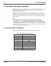
Table 4-1: Summary of Power-On/Reset Options
S1D13505
Pin Name
value on this pin at rising edge of RESET# is used to configure:
(1/0)
10
MD0 8-bit host bus interface
16-bit host bus interface
MD[3:1] 101 = MIPS/ISA bus interface
MD4 Little Endian Big Endian
MD5 WAIT# is active high (1 = insert wait state)
WAIT# is active low (0 = insert wait state)
MD11 Alternate Host Bus Interface Selected
Primary Host Bus Interface Selected
= configuration for NEC VR4102/VR4111 microprocessor