


Page 14
Epson Research and Development
Vancouver Design Center
S1D13505 Interfacing to the Motorola MPC821 Microprocessor
X23A-G-008-05 Issue Date: 01/02/05
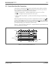
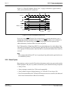
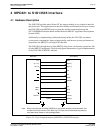
3.2 PowerPC Host Bus Interface Signals
The interface requires the following signals:
• BUSCLK is a clock input which is required by the S1D13505 host bus interface. It is
separate from the input clock (CLKI) and is typically driven by the host CPU system
clock.
• The address inputs AB[20:0], and the data bus DB[15:0], connect directly to the
PowerPC bus address (A[11:31]) and data bus (D[0:15]), respectively. MD4 must be set
to select the proper endian mode upon reset.
• M/R# (memory/register) selects between memory or register access. It may be
connected to an address line, allowing system address A10 to be connected to the M/R#
line.
• Chip Select (CS#) must be driven low whenever the S1D13505 is accessed by the
PowerPC bus.
• RD/WR# connects to RD/WR
which indicates whether a read or a write access is being
performed on the S1D13505.
• WE1# connects to BI
(burst inhibit signal). WE1# is output by the S1D13505 to indicate
whether the S1D13505 is able to perform burst accesses.
• WE0# and RD# connect to TSIZ1 and TSIZ0 (high and low byte enable signals). These
signals must be driven by the PowerPC bus to indicate the size of the transfer taking
place on the bus.
• WAIT# connects to TA
and is output from the S1D13505 that indicates the PowerPC
bus must wait until data is ready (read cycle) or accepted (write cycle) on the host bus.
Since the PowerPC bus accesses to the S1D13505 may occur asynchronously to the
display update, it is possible that contention may occur in accessing the S1D13505
internal registers and/or display buffer. The WAIT# line resolves these contentions by
forcing the host to wait until the resource arbitration is complete.
• The Bus Start (BS#) signal connects to TS
(the transfer start signal).