


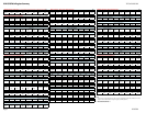

S1D13505F00A Register Summary X23A-R-001-04
Page 1 01/02/06
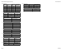
Notes
1 These bits are used to identify the S1D13505. For the S1D13505 the product code should be 3. The host
interface must be enabled before reading this register (set REG[1B] b7=0).
2 N/A bits should be written 0.
Reserved bits must be written 0.
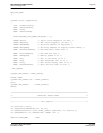
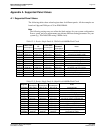
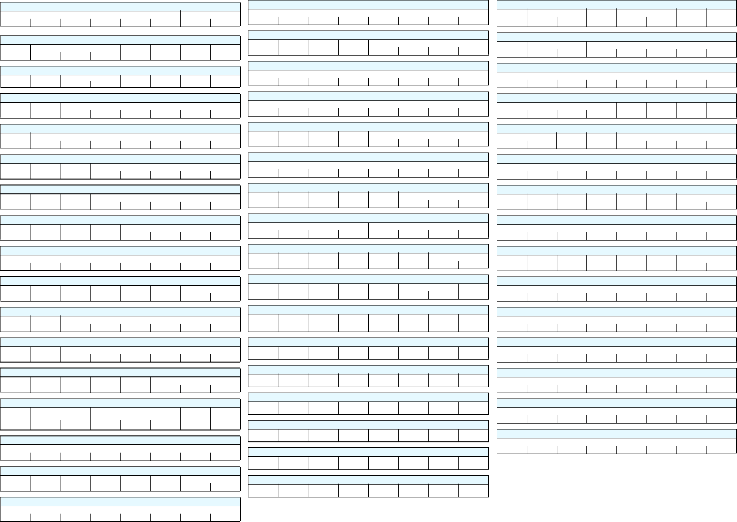
REG[00h] R
EVISION
C
ODE
R
EGISTER
1
(For S1D13505: Product Code=000011b, Revision Code=00b)RO
Product Code Revision Code
Bit 5 Bit 4 Bit 3 Bit 2 Bit 1 Bit 0 Bit 1 Bit 0
REG[01h] M
EMORY
C
ONFIGURATION
R
EGISTER
1/0 RW
n/a
2
Refresh Rate
3
n/a WE# Control n/a
Memory
Type
Bit 2 Bit 1 Bit 0
REG[02h] P
ANEL
T
YPE
R
EGISTER
1/0 RW
EL Panel
Enable
n/a
Panel Data Width
4
Panel Data
Format Slct
Color/Mono
Panel Slct
Dual/Single
Panel Slct
TFT/Passive
LCD Pan Slct
Bit 1 Bit 0
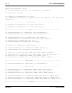
REG[03h] M
OD
R
ATE
R
EGISTER
RW
n/a n/a
MOD Rate
Bit 5 Bit 4 Bit 3 Bit 2 Bit 1 Bit 0
REG[04h] H
ORIZONTAL
D
ISPLAY
W
IDTH
R
EGISTER
RW
n/a
Horizontal Display Width = 8(REG + 1)
Bit 6 Bit 5 Bit 4 Bit 3 Bit 2 Bit 1 Bit 0
REG[05h] H
ORIZONTAL
N
ON
-D
ISPLAY
P
ERIOD
R
EGISTER
RW
n/a n/a n/a
Horizontal Non-Display Period = 8(REG + 1)
Bit 4 Bit 3 Bit 2 Bit 1 Bit 0
REG[06h] HRTC/FPLINE S
TART
P
OSITION
R
EGISTER
RW
n/a n/a n/a
HRTC/FPLINE Start Position = 8(REG + 1) - 2
Bit 4 Bit 3 Bit 2 Bit 1 Bit 0
REG[07h] HRTC/FPLINE P
ULSE
W
IDTH
R
EGISTER
RW
HRTC
Polarity Slct
FPLINE
Polarity Slct
n/a n/a
HRTC/FPLINE Pulse Width = 8(REG + 1)
Bit 3 Bit 2 Bit 1 Bit 0
REG[08h] V
ERTICAL
D
ISPLAY
H
EIGHT
R
EGISTER
0 RW
Vertical Display Height = (REG + 1)
Bit 7 Bit 6 Bit 5 Bit 4 Bit 3 Bit 2 Bit 1 Bit 0
REG[09h] V
ERTICAL
D
ISPLAY
H
EIGHT
R
EGISTER
1 RW
n/a n/a n/a n/a n/a n/a
Vertical Display Height
Bit 9 Bit 8
REG[0Ah] V
ERTICAL
N
ON
-D
ISPLAY
P
ERIOD
R
EGISTER
RW
VNDP
Status (RO)
n/a
Vertical Non-Display Period (VNDP) = (REG + 1)
Bit 5 Bit 4 Bit 3 Bit 2 Bit 1 Bit 0
REG[0Bh] VRTC/FPFRAME S
TART
P
OSITION
R
EGISTER
RW
n/a n/a
VRTC/FPFRAME Start Position = (REG + 1)
Bit 5 Bit 4 Bit 3 Bit 2 Bit 1 Bit 0
REG[0Ch] VRTC/FPFRAME P
ULSE
W
IDTH
R
EGISTER
RW
VRTC
Polarity Slct
FPFRAME
Polarity Slct
n/a n/a n/a
VRTC/FPFRAME Pulse Width = (REG + 1)
Bit 2 Bit 1 Bit 0
REG[0Dh] D
ISPLAY
M
ODE
R
EGISTER
RW
Hardware
Portrait
Mode
Enable
Simultaneous Display
5
Option Select
Bit-per-pixel Select
6
CRT Enable LCD Enable
Bit 1 Bit 0 Bit 2 Bit 1 Bit 0
REG[0Eh] S
CREEN
1 L
INE
C
OMPARE
R
EGISTER
0 RW
Screen 1 Line Compare
Bit 7 Bit 6 Bit 5 Bit 4 Bit 3 Bit 2 Bit 1 Bit 0
REG[0Fh] S
CREEN
1 L
INE
C
OMPARE
R
EGISTER
1 RW
n/a n/a n/a n/a n/a n/a
Screen 1 Line Compare
Bit 9 Bit 8
REG[10h] S
CREEN
1 D
ISPLAY
S
TART
A
DDRESS
R
EGISTER
0 RW
Screen 1 Start Address
Bit 7 Bit 6 Bit 5 Bit 4 Bit 3 Bit 2 Bit 1 Bit 0
REG[11h] S
CREEN
1 D
ISPLAY
S
TART
A
DDRESS
R
EGISTER
1 RW
Screen 1 Start Address
Bit 15 Bit 14 Bit 13 Bit 12 Bit 11 Bit 10 Bit 9 Bit 8
REG[12h] S
CREEN
1 D
ISPLAY
S
TART
A
DDRESS
R
EGISTER
2 RW
n/a n/a n/a n/a
Screen 1 Start Address
Bit 19 Bit 18 Bit 17 Bit 16
REG[13h] S
CREEN
2 D
ISPLAY
S
TART
A
DDRESS
R
EGISTER
0 RW
Screen 2 Start Address
Bit 7 Bit 6 Bit 5 Bit 4 Bit 3 Bit 2 Bit 1 Bit 0
REG[14h] S
CREEN
2 D
ISPLAY
S
TART
A
DDRESS
R
EGISTER
1 RW
Screen 2 Start Address
Bit 15 Bit 14 Bit 13 Bit 12 Bit 11 Bit 10 Bit 9 Bit 8
REG[15h] S
CREEN
2 D
ISPLAY
S
TART
A
DDRESS
R
EGISTER
2 RW
n/a n/a n/a n/a
Screen 2 Start Address
Bit 19 Bit 18 Bit 17 Bit 16
REG[16h] M
EMORY
A
DDRESS
O
FFSET
R
EGISTER
0 RW
Memory Address Offset
Bit 7 Bit 6 Bit 5 Bit 4 Bit 3 Bit 2 Bit 1 Bit 0
REG[17h] M
EMORY
A
DDRESS
O
FFSET
R
EGISTER
1 RW
n/a n/a n/a n/a n/a
Memory Address Offset
Bit 10 Bit 9 Bit 8
REG[18h] P
IXEL
P
ANNING
R
EGISTER
RW
Screen 2 Pixel Panning Screen 1 Pixel Panning
Bit 3 Bit 2 Bit 1 Bit 0 Bit 3 Bit 2 Bit 1 Bit 0
REG[19h] C
LOCK
C
ONFIGURATION
R
EGISTER
RW
Reserved n/a n/a n/a n/a
MCLK
Divide Slct
PCLK Divide
7
Slct
Bit 1 Bit 0
REG[1Ah] P
OWER
S
AVE
C
ONFIGURATION
R
EGISTER
RW
Power Save
Status RO
n/a n/a n/a
LCD Power
Disable
Suspend Refresh Select
8
Software
Suspend En
Bit 1 Bit 0
REG[1Bh] M
ISCELLANIOUS
R
EGISTER
RW
Host
Interface
Disable
n/a n/a n/a n/a n/a n/a
Half Frame
Buffer
Disable
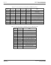
REG[1Ch] MD C
ONFIGURATION
R
EADBACK
R
EGISTER
0 RO
MD7
Status
MD6
Status
MD5
Status
MD4
Status
MD3
Status
MD2
Status
MD1
Status
MD0
Status
REG[1Dh] MD C
ONFIGURATION
R
EADBACK
R
EGISTER
1 RO
MD15
Status
MD14
Status
MD13
Status
MD12
Status
MD11
Status
MD10
Status
MD9
Status
MD8
Status
REG[1Eh] G
ENERAL
IO P
INS
C
ONFIGURATION
R
EGISTER
0 RW
n/a n/a n/a n/a
GPIO3 Pin
IO Config
GPIO2 Pin
IO Config
GPIO1 Pin
IO Config
n/a
REG[1Fh] G
ENERAL
IO P
INS
C
ONFIGURATION
R
EGISTER
1 RW
n/a n/a n/a n/a n/a n/a n/a n/a
REG[20h] G
ENERAL
IO P
INS
C
ONTROL
R
EGISTER
0 RW
n/a n/a n/a n/a
GPIO3 Pin
IO Status
GPIO2 Pin
IO Status
GPIO1 Pin
IO Status
n/a
REG[21h] G
ENERAL
IO P
INS
C
ONTROL
R
EGISTER
1 RW
GPO
Control
n/a n/a n/a n/a n/a n/a n/a
REG[22h] P
ERFORMANCE
E
NHANCEMENT
R
EGISTER
0 RW
Reserved
RC Timing Value
9
RAS#-to-
CAS#
Delay
10
RAS# Precharge
11
Timing
Reserved Reserved
Bit 1 Bit 0 Bit 1 Bit 0
REG[23h] P
ERFORMANCE
E
NHANCEMENT
R
EGISTER
1 RW
Display FIFO
Disable
CPU to Memory Wait State Display FIFO Threshold
Bit 1Bit 0Bit 4Bit 3Bit 2Bit 1Bit 0
REG[24h] L
OOK
-U
P
T
ABLE
A
DDRESS
R
EGISTER
RW
Look-Up Table Address
Bit 7Bit 6Bit 5Bit 4Bit 3Bit 2Bit 1Bit 0
REG[26h] L
OOK
-U
P
T
ABLE
D
ATA
R
EGISTER
RW
Look-Up Table Data
n/a n/a n/a n/a
Bit 3Bit 2Bit 1Bit 0
REG[27h] I
NK
/C
URSOR
C
ONTROL
R
EGISTER
RW
Ink/Cursor Mode
n/a n/a
Cursor High Threshold
Bit 1Bit 0 Bit 3Bit 2Bit 1Bit 0
REG[28h] C
URSOR
X P
OSITION
R
EGISTER
0 RW
Cursor X Position
Bit 7Bit 6Bit 5Bit 4Bit 3Bit 2Bit 1Bit 0
REG[29h] C
URSOR
X P
OSITION
R
EGISTER
1 RW
Reserved n/a n/a n/a n/a n/a
Cursor X Position
Bit 9 Bit 8
REG[2Ah] C
URSOR
Y P
OSITION
R
EGISTER
0 RW
Cursor Y Position
Bit 7Bit 6Bit 5Bit 4Bit 3Bit 2Bit 1Bit 0
REG[2Bh] C
URSOR
Y P
OSITION
R
EGISTER
1 RW
Reserved n/a n/a n/a n/a n/a
Cursor Y Position
Bit 9 Bit 8
REG[2Ch] I
NK
/C
URSOR
C
OLOR
0 R
EGISTER
0 RW
Cursor Color 0
Bit 7Bit 6Bit 5Bit 4Bit 3Bit 2Bit 1Bit 0
REG[2Dh] I
NK
/C
URSOR
C
OLOR
0 R
EGISTER
1 RW
Cursor Color 0
Bit 15 Bit 14 Bit 13 Bit 12 Bit 11 Bit 10 Bit 9 Bit 8
REG[2Eh] I
NK
/C
URSOR
C
OLOR
1 R
EGISTER
0 RW
Cursor Color 1
Bit 7Bit 6Bit 5Bit 4Bit 3Bit 2Bit 1Bit 0
REG[2Fh] I
NK
/C
URSOR
C
OLOR
1 R
EGISTER
1 RW
Cursor Color 1
Bit 15 Bit 14 Bit 13 Bit 12 Bit 11 Bit 10 Bit 9 Bit 8
REG[30h] I
NK
/C
URSOR
S
TART
A
DDRESS
S
ELECT
R
EGISTER
RW
Ink/Cursor Start Address Select
12
Bit 7 WOBit 6Bit 5Bit 4Bit 3Bit 2Bit 1Bit 0
REG[31h] A
LTERNATE
FRM R
EGISTER
RW
Alternate Frame Range Modulation Select
Bit 7Bit 6Bit 5Bit 4Bit 3Bit 2Bit 1Bit 0
S1D13505F00A Register Summary