


Page 10
Epson Research and Development
Vancouver Design Center
S1D13505 Interfacing to the Motorola MPC821 Microprocessor
X23A-G-008-05 Issue Date: 01/02/05
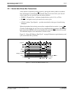
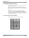
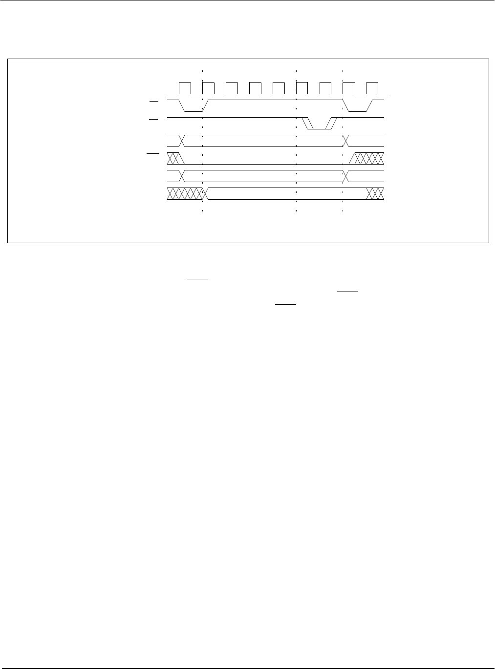
Figure 2-2: “Power PC Memory Write Cycle” on page 10 illustrates a typical memory
write cycle on the Power PC system bus.
Figure 2-2: Power PC Memory Write Cycle
If an error occurs, TEA
(Transfer Error Acknowledge) is asserted and the bus cycle is
aborted. For example, a peripheral device may assert TEA
if a parity error is detected, or
the MPC821 bus controller may assert TEA
if no peripheral device responds at the
addressed memory location within a bus time-out period.
For 32-bit transfers, all data lines (D[0:31]) are used and the two low-order address lines
A30 and A31 are ignored. For 16-bit transfers, data lines D[0:15] are used and address line
A31 is ignored. For 8-bit transfers, data lines D[0:7] are used and all address lines (A[0:31])
are used.
Note
This assumes that the Power PC core is operating in big endian mode (typically the case
for embedded systems).
2.2.2 Burst Cycles
Burst memory cycles are used to fill on-chip cache memory and to carry out certain on-chip
DMA operations. They are very similar to normal bus cycles with the following exceptions:
• Always 32-bit.
• Always attempt to transfer four 32-bit words sequentially.
• Always address longword-aligned memory (i.e. A30 and A31 are always 0:0).
• Do not increment address bits A28 and A29 between successive transfers; the addressed
device must increment these address bits internally.
A[0:31]
D[0:31]
TSIZ[0:1], AT[0:3]
TS
TA
SYSCLK
Wait StatesTransfer Start
RD/WR
Valid
Transfer Next Transfer
Complete Starts